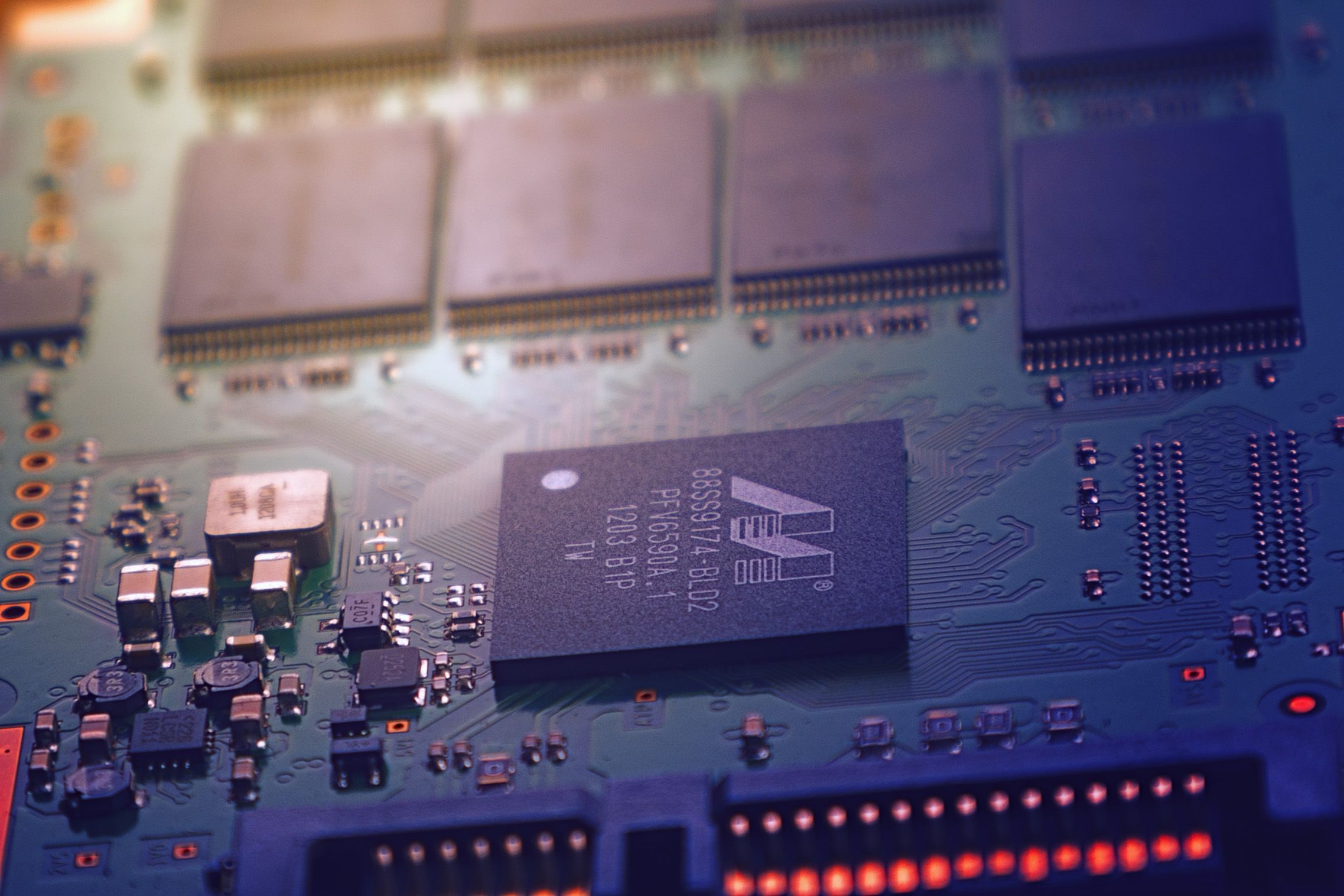
Xanadu Quantum Technologies (NASDAQ/TSX: XNDU) announced on October 6 that it has signed a strategic multi-year manufacturing partnership with GlobalFoundries (GF) to produce the two core hardware components of its fault-tolerant photonic quantum computers — ultra-low-loss silicon nitride optical circuits and superconducting nanowire single-photon detectors (SNSPDs) — on GF’s 300mm commercial wafer line in Malta, New York. This is the moment photonic quantum hardware crosses from the world of specialized research fabs and university clean rooms into the same factory floors that already produce semiconductors by the billions.
For the technically literate reader, that sentence is not rhetorical shorthand. It is a description of a specific and previously unsolved engineering transition: the challenge of integrating nanoscale superconducting films and ultra-low-loss glass-like nitride waveguides into a standard industrial process flow — and doing it reliably, at 300mm wafer scale, in a facility already operating one of the world’s most advanced photonics manufacturing platforms.
What a Photonic Quantum Computer Actually Needs From a Factory
Photonic quantum computers encode information in photons — individual particles of light — rather than in the electrons of classical chips, the superconducting circuits cooled to millikelvin temperatures by IBM and Google, or the trapped ions levitated under vacuum by IonQ and Quantinuum. The fundamental advantage of the photonic approach is that light naturally maintains its quantum state far longer than matter-based qubits: photons decohere more slowly because they do not readily interact with their environment.
But that advantage comes with an engineering price. If even a small fraction of photons are lost in transit — absorbed by the waveguide material, scattered by surface imperfections, or missed by the detector — the quantum information they carried is simply gone, without the possibility of recovery. In Xanadu’s architecture, photon loss is not one error source among many: it is the primary error source, and reducing it to a sufficiently low threshold is the single prerequisite for reaching fault-tolerant operation according to the company’s August 2026 roadmap.
This is why two specific components are the focus of the GF partnership.
Silicon nitride (SiN) waveguides function as the optical circuit boards of Xanadu’s quantum chips. Silicon nitride — the chemical compound Si₃N₄, a material more familiar as an industrial ceramic — produces ultra-low-loss SiN waveguides because of its wide optical transparency window and extremely low absorption at the wavelengths Xanadu uses. When fabricated with careful process control, SiN waveguides can guide photons across a chip with negligible loss, allowing the quantum states to survive the routing, mixing, and interference operations that constitute photonic quantum computation. Critically for Xanadu’s architecture, SiN also supports the generation of “squeezed states” of light — quantum states whose noise properties have been shaped below the classical limit — which are the raw material from which Xanadu builds its error-correctable GKP qubits.
Silicon nitride is distinct from the silicon photonics platform that competitor PsiQuantum uses with GF at the same Malta fab. Silicon waveguides suffer from two-photon absorption in silicon at the power levels and wavelengths needed for quantum operations; silicon nitride does not, making SiN the material of choice for low-loss photonic quantum computing even though it requires different process chemistry and tooling.
Superconducting nanowire single-photon detectors (SNSPDs) are the eyes of the system — the sensors that read out the result of a quantum calculation by detecting individual photons, one at a time, with extraordinary timing precision. The mechanism is elegant in its physics: a superconducting nanowire single-photon detector roughly 5 nanometers (0.0000002 inches) thick and 100 nanometers (0.000004 inches) wide is cooled to approximately 1–4 Kelvin (−457°F to −452°F, or about 39°F to 7°F above absolute zero) and biased just below the maximum current it can carry while remaining superconducting. When a single photon strikes the wire, it deposits enough energy to break the Cooper-pair hotspot detection superconducting state at that point, creating a tiny resistive “hotspot.” The bias current can no longer flow without resistance, so it is shunted to a readout circuit, producing a measurable voltage pulse that registers the photon’s arrival within approximately 3–10 picoseconds. Within nanoseconds, the hotspot cools and the nanowire returns to its superconducting state, ready to detect the next photon.
As of 2026, SNSPDs are the fastest single-photon detectors available, and their SNSPD detection efficiency exceeds 98% at the telecom wavelengths Xanadu uses — meaning fewer than two in a hundred photons are missed. That near-perfect efficiency is what makes them architecturally essential. Xanadu’s error-correction scheme — which pairs GKP (Gottesman-Kitaev-Preskill) encoding of individual photonic qubits with an outer quantum low-density parity-check (qLDPC) code — requires GKP photon-number-resolving detection: the ability to determine not merely whether a photon arrived, but precisely how many photons arrived in a single light pulse.
The standard SNSPD achieves photon-number-resolving capability through arrays of nanowire segments with advanced readout schemes. According to Xanadu, adopting SNSPDs is expected to dramatically increase the speed of its quantum computing systems and substantially reduce the chip overhead required to reach utility-scale performance.
One Critical Clarification on Cryogenic Requirements
The photonic processing layer of Xanadu’s architecture — the SiN waveguides, the beamsplitters, the phase shifters, and the fiber optics connecting the server racks — does operate at room temperature. Photons travel without cryogenic assistance through the optical circuits. This is a genuine and significant engineering advantage: IBM’s and Google’s quantum processors must be cooled to roughly 15 millikelvin (approximately −459.6°F, or 0.015 degrees above absolute zero) inside dilution refrigerators, limiting how many systems can be deployed and how they can be integrated with conventional data center infrastructure.
But the SNSPDs used to read out Xanadu’s photonic computation do require cryogenic cooling — to the 1–4 K range achievable with liquid helium or modern closed-cycle cryocoolers. MIT Technology Review Aurora coverage from January 2025 noted that Aurora’s “server racks operate at room temperature, although photon-counting detectors still need to be cryogenically cooled in another room.” That is far less extreme than millikelvin dilution refrigeration, and the cooling subsystem occupies a separate room from the main computing racks rather than being embedded inside each server — but it is cooling nonetheless. The correct framing is: Xanadu’s architecture eliminates the most operationally challenging cryogenic requirement (millikelvin dilution refrigeration) while retaining a manageable one (standard 4 K cooling, the same regime used in MRI machines and particle physics experiments). Readers planning quantum infrastructure should understand this distinction.
How 300mm Wafer Manufacturing Changes the Economics
Research-grade photonic components are typically fabricated in small batches on 100mm (3.94 inch) or 150mm (5.91 inch) wafers, in university clean rooms or specialized photonics facilities. The yields are often modest, the process tolerances are manually tuned, and the throughput is measured in tens of wafers per month. None of this is adequate for a fault-tolerant quantum system that may require hundreds of photonic chips to assemble even a modest number of logical qubits.
A 300mm wafer economics explained means a 300mm (11.8 inch) wafer has 2.25 times the area of a 200mm (7.87 inch) wafer, with roughly comparable per-wafer capital and operating cost. That ratio translates directly into lower cost per component and higher throughput per fab run — the same economic logic that drove the classical semiconductor industry’s migration from 200mm to 300mm in the early 2000s. For Xanadu, whose Aurora system — described in its Aurora Nature paper January 2025 in Nature — required 35 photonic chips to implement 12 qubits across four interconnected server racks connected by 13 kilometers (8.1 miles) of fiber optics, scaling to the hundreds or thousands of logical qubits it targets by 2029–2031 demands exactly the kind of industrial throughput that only a 300mm commercial fab can provide.
GF’s Malta fab is not a generic semiconductor factory being pressed into service for quantum hardware. Since 2021, it has been manufacturing silicon photonic chipsets for PsiQuantum, Xanadu’s primary competitor in the photonic quantum computing space, through a PsiQuantum-GF silicon photonics partnership that preceded Xanadu’s manufacturing transition. GF launched its dedicated Quantum Technology Solutions (QTS) business unit in May 2026, and finalized a $375 million CHIPS Act QTS award from the U.S. Department of Commerce’s CHIPS Research and Development Office on September 8, 2026, specifically to expand its quantum semiconductor manufacturing capabilities. The same fab facility also holds a separate $300 million silicon photonics LOI from Commerce for silicon photonics R&D.
For Xanadu, signing with GF is not just a manufacturing decision — it is a co-location with the quantum photonics manufacturing ecosystem that US federal policy is now actively capitalizing.
From Lab Result to Factory Product: The 2025 Nature Paper
The Xanadu–GF partnership did not emerge from a standing start. In June 2025, Xanadu published a landmark result in the journal Nature: the first-ever generation of a GKP qubit state directly on an integrated silicon nitride chip, fabricated on a 300mm wafer platform. The Xanadu GKP on-chip Nature paper integrated squeezed-state generation, linear optical manipulation, and photon-number-resolving detectors with greater than 99% efficiency, demonstrating that all three components could be fabricated on a single platform suitable for commercial wafer-scale manufacturing.
“GKP states are, in a sense, the optimal photonic qubit, since they enable logic gates and error correction at room temperature and using relatively straightforward, deterministic operations,” said Zachary Vernon, CTO of Hardware at Xanadu, at the time. The result validated that Xanadu’s choice of SiN as its photonic material — and the specific process chemistry required to fabricate ultra-low-loss SiN waveguides — was transferable to a commercial 300mm wafer environment, at least at the research quantity level. The GF partnership now tasks both companies with transferring that process chemistry into GF’s industrial production flow, where it must be stable, reproducible, and high-yield at commercial volumes.
The specific manufacturing challenge is non-trivial. Integrating the NbN or NbTiN superconducting metal layer required for SNSPDs into a standard CMOS-compatible 300mm process flow means introducing a superconducting thin-film deposition step that must not contaminate the facility’s standard silicon and oxide layers. Every process step that follows must remain compatible with the properties of the superconducting film. The two companies have described this integration work as an active area of their collaboration, with additional “future work packages” for high-performance quantum modules beyond the initial SiN and SNSPD scope.
Industry Context: One Fab, Two Competing Architectures
The GF Malta complex now finds itself at the center of a race that most of the semiconductor industry did not anticipate would consolidate so quickly around a single foundry location.
PsiQuantum, the Palo Alto-based photonic quantum computing company widely considered Xanadu’s closest competitor, has been manufacturing silicon photonic chipsets at GF Malta since 2021. PsiQuantum’s approach uses discrete single photons as its basic quantum information unit — a “dual-rail” qubit architecture — rather than Xanadu’s continuous-variable approach using squeezed states. The two architectures require different materials (silicon versus silicon nitride), different photon sources, and different detector configurations. Yet both companies have now chosen GF Malta as their path from laboratory to industrial production, as described in the PsiQuantum silicon photonics approach published in a 2024 Nature paper.
That co-location makes GF Malta something unprecedented: the single global factory producing hardware for two competing approaches to the hardest engineering challenge in commercial quantum computing. The strategic implications cut both ways. For the quantum industry, the concentration validates the bet that commercial semiconductor manufacturing is the right path to fault-tolerant quantum hardware. For national security planners and risk analysts, a single facility being the primary locus for both leading photonic quantum architectures represents a concentration of critical supply-chain dependency that is worth noting.
In an October 6 statement, Nicholas Sergeant, VP of Quantum Technology Solutions at GF, said the partnership “creates a path to industrialize the critical components needed to accelerate the deployment of fault-tolerant systems and enable future quantum computing architectures.”
Dr. Christian Weedbrook, Xanadu’s Founder and CEO, framed the deal in terms of execution rather than invention: “Transitioning quantum computing technology to a high-volume manufacturing line is fundamental to delivering quantum computing at scale. Partnering with GlobalFoundries allows Xanadu to refine and scale up our existing industry-leading photonics platform and apply GF’s industrial expertise and technology to our photonic chip production.” Both quotes appear in the Xanadu-GF partnership press release.
What the Roadmap Now Requires
Xanadu presented an expanded technology roadmap to investors on August 31, 2026. The headline targets are fault-tolerant operation by 2028–2029, a quantum data center deployment of up to 200 logical qubits by 2029–2030, and commercial utility scaling to more than 1,000 logical qubits by 2031. The Xanadu August 2026 roadmap details a specific metric that governs whether those targets are achievable: the company’s “loss ratio,” currently measured at 24.1x the threshold required for fault-tolerant operation, which must be reduced to 1.0x by 2030. Projected logical error rates improve from 10⁻³–10⁻⁸ at initial fault tolerance in 2028–2029, targeting 10⁻¹⁶ by 2030.
That loss ratio is the single most important number in photonic quantum computing — and it is exactly the quantity that SiN waveguide quality and SNSPD efficiency most directly determine. A higher-quality SiN process reduces propagation loss in the waveguides; a higher-efficiency SNSPD reduces the fraction of computation-ending photon-loss events at readout. The GF partnership is, at its core, a manufacturing commitment to close that 24.1x gap according to the same roadmap.
Isaac Kim, a physicist at the University of California, Davis, noted in early 2025 that Xanadu had not yet demonstrated the error-correction capability many experts consider essential before a quantum computer can perform genuinely useful tasks — meaning the gap between Aurora’s demonstration of modularity and fault-tolerant utility was still substantial, according to MIT Technology Review Xanadu critique. The GF manufacturing partnership represents Xanadu’s answer to that critique: the path from loss ratio 24.1x to 1.0x runs through industrial-scale SiN and SNSPD production, not through further laboratory experiments.
Xanadu is simultaneously building a 158,000-square-foot manufacturing facility in Toronto for testing, chip integration, and rack-level module assembly. The federal government of Canada signed a definitive agreement for CAD $195 million toward the project — the federal portion of a potential total of up to CAD $390 million in Xanadu Toronto manufacturing facility support, with negotiations for the Ontario provincial portion ongoing. The company’s Xanadu $686 million capital resources stood at approximately $686 million as of June 30, 2026.
XNDU rose 17% on announcement day, October 6, on the partnership announcement, while GF shares gained roughly 1.4% on the same day.
Whether any photonic quantum system reaches commercial fault tolerance on its developer’s stated timeline is a question no independent analyst has yet answered definitively. What the Xanadu–GF partnership establishes concretely is that the manufacturing infrastructure for the attempt is now being assembled in the same New York state fab complex that already anchors America’s photonics semiconductor ecosystem — and that the US government, through its CHIPS Act quantum allocations, has placed a $375 million bet on the same address.
Frequently Asked Questions
How does Xanadu’s photonic quantum computer differ from IBM’s or Google’s?
IBM and Google build quantum processors from superconducting circuits that must be cooled to roughly 15 millikelvin — about 0.015 degrees above absolute zero — inside dilution refrigerators. Xanadu’s approach uses photons (particles of light) traveling through silicon nitride waveguides to carry quantum information, with the computation itself occurring at room temperature. The photon-counting detectors still require cooling to the 1–4 Kelvin range (about −457°F to −452°F), achievable with standard liquid-helium cryocoolers rather than the more complex dilution refrigerators, making the system potentially more compatible with conventional data center infrastructure. The tradeoff is that photonic architectures are highly sensitive to photon loss, which is the primary engineering challenge Xanadu is working to solve.
What is a superconducting nanowire single-photon detector and why does it matter for quantum computing?
An SNSPD is a sensor made from a nanoscale superconducting wire, cooled to near absolute zero, that can detect a single photon with greater than 98% efficiency and resolve its arrival time to within a few picoseconds. In Xanadu’s architecture, reading out the result of a quantum calculation requires knowing exactly how many photons arrived in a light pulse — not just whether one arrived. SNSPDs are the only detector technology that can do this reliably and quickly enough to keep pace with the quantum computation. Their integration into a 300mm commercial wafer process, which this GF partnership targets, is one of the key manufacturing milestones between current photonic quantum systems and fault-tolerant operation.
What does “fault-tolerant” quantum computing mean, and when will it arrive?
A fault-tolerant quantum computer is one that can correct its own errors faster than new errors accumulate, allowing calculations to run for long enough to produce useful results. Current quantum computers — including Xanadu’s Aurora system — make errors at a rate that limits them to short circuits before errors overwhelm the computation. Xanadu’s error-correction strategy uses GKP-encoded photonic qubits (which can self-correct small errors) paired with an outer qLDPC code (which handles residual errors across multiple qubits). The company’s August 2026 roadmap targets fault-tolerant operation by 2028–2029, requiring its loss ratio to fall from the current 24.1x above the fault-tolerance threshold to 1.0x. Independent physicists have noted that this goal remains ambitious and has not yet been experimentally demonstrated — but the GF manufacturing partnership is designed to provide the industrial-quality hardware needed to attempt it.
Is Malta, New York becoming the global hub for photonic quantum chip manufacturing?
Effectively, yes — for now. GlobalFoundries’ Malta fab is already producing silicon photonic chipsets for PsiQuantum, Xanadu’s closest competitor, and will now also produce silicon nitride photonics and SNSPD components for Xanadu. The US Department of Commerce has invested $375 million in GF’s dedicated Quantum Technology Solutions business unit at the same site, accelerating its capacity to support multiple quantum hardware companies. The concentration of two competing photonic quantum architectures at a single commercial fab is historically unusual and reflects both the specialized capabilities GF has built in photonics manufacturing and the active US federal effort to consolidate domestic quantum hardware production in a single, secure facility.