HomeAuto ORNL Commissions Sub-Ångström Microscope to Drive Autonomous Materials Discovery
ORNL Commissions Sub-Ångström Microscope to Drive Autonomous Materials Discovery
October 28, 2026:
Ornl.gov
Oak Ridge National Laboratory has installed one of the most capable aberration-corrected electron microscopes in the US national laboratory system — and the instrument is designed from the outset not merely to see individual atoms but to eventually direct its own experiments, building the statistical datasets that materials discovery at speed requires.
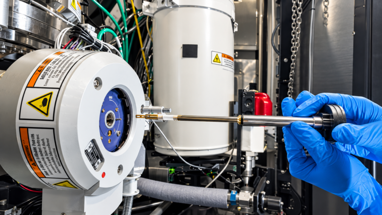
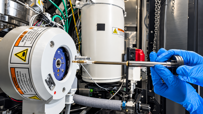
The new instrument, a Thermo Scientific Spectra Ultra scanning transmission electron microscope (STEM), is now operational in ORNL’s Advanced Microscopy Laboratory. The announcement, made October 26, 2026, places the facility among an elite group capable of imaging matter at sub-ångström scales — below 0.05 nanometers (about 0.002 millionths of an inch), small enough to distinguish individual atoms within a crystal lattice and then map the chemical identity of each one in the same experiment.
What makes the commissioning more than an instrumentation upgrade is the context around the hardware. ORNL’s team is actively developing Super Intelligence (SI)-enabled autonomous workflows — systems that use machine learning to steer the electron beam, collect and evaluate data, and identify microstructural features of interest without continuous human input. Prior generations of STEM produced individual atomic-scale observations; the Spectra Ultra, integrated with ORNL’s existing AI frameworks, is designed to systematically process large sample libraries, building statistical maps of microstructure-property relationships across entire material families. The shift is from precision observation to automated atomic-scale data mining — and the rate of materials discovery changes accordingly.
What Aberration Correction Actually Does — and Why It Matters
A scanning transmission electron microscope builds its image by raster-scanning a finely focused beam of electrons across an ultra-thin sample, typically 50–100 nanometers (0.002–0.004 thousandths of an inch) thick, and detecting how those electrons scatter. The limiting factor has historically been spherical aberration: round magnetic lenses inevitably blur the electron beam at its edges, restricting how tightly the probe can be focused. Otto Scherzer demonstrated in 1936 that this is a fundamental consequence of lens geometry, not a manufacturing defect — making it an engineering problem with no simple fix, as detailed in the history of aberration-corrected electron microscopy.
Richard Feynman implicitly identified the challenge in his famous 1959 lecture There’s Plenty of Room at the Bottom, calling explicitly for a 100-fold improvement in electron microscope resolution by overcoming spherical aberration. Practical correctors — using multipole magnetic elements whose fields offset the aberrating effects of the main objective lens — only became feasible in the 1990s when real-time computational wavefront analysis caught up with the hardware. ORNL was part of that breakthrough: researchers there, working with Nion Co. of Kirkland, Washington, produced world-record aberration-corrected STEM images as early as 2004, demonstrating 0.6 ångström (0.06 nm) resolution at a time when 1.3 ångström had been the state of the art.
The Spectra Ultra carries two independent aberration correctors: the S-CORR for the electron probe (the illuminating beam), and the CETCOR for the imaging lens. Together they eliminate both the spherical distortion that blurs the probe and the residual geometric aberrations in the image-forming optics, enabling the 50-picometer spatial resolution ORNL’s team will routinely work at.
Three Technical Capabilities That Distinguish This Instrument
Energy resolution at the atomic scale. Conventional STEM instruments produce an electron beam with an energy spread of roughly 1 electron volt — wide enough to smear out the fine spectroscopic signals that reveal bond type and oxidation state. The Spectra Ultra is configured with an X-FEG/UltiMono monochromator that narrows that spread to below 0.025 electronvolts at 60 kilovolt operating voltage. That level of energy resolution enables vibrational spectroscopy inside the electron microscope — detecting the specific bond-stretching and bending modes that identify chemical species — a capability that was confined to optical labs until recently.
Variable accelerating voltage. Most high-end STEM instruments operate at a fixed voltage, typically 200 or 300 kilovolts. The Spectra Ultra’s S-TWIN Prime objective lens uses a ConstantPower design that keeps the lens thermally stable while the accelerating voltage is switched rapidly between 30 and 300 kilovolts. Lower voltages reduce beam damage to electron-sensitive materials — organic compounds, two-dimensional materials like graphene, lithium-containing battery electrode materials. Higher voltages improve penetration in thicker samples and increase contrast in heavy-element alloys. The result is a single instrument with the range to study the entire portfolio of materials ORNL’s programs require, from exotic quantum materials to workhorse automotive alloys.
The 16-segment Panther detector. Traditional STEM imaging uses a single annular ring detector that captures electrons scattered to high angles, producing the high-angle annular dark-field (HAADF) signal sensitive to atomic-number contrast. The Panther system replaces that with two solid-state, eight-segment ring-and-disk detectors totaling 16 independent channels. By comparing the signal across segments, researchers can perform differential phase contrast imaging — a technique sensitive to weak electric fields inside a material, revealing the charge redistribution at grain boundaries and interfaces that govern corrosion resistance, magnetic switching, and catalytic activity. These are features invisible in conventional HAADF images.
Where the Science Goes: Alloys, Magnets, Catalysts, and Quantum Materials
The four research priorities ORNL named reflect both the instrument’s capabilities and the federal funding behind it.
Lightweight automotive alloys. ORNL’s Powertrain Materials Core Program, a DOE consortium, studies why high-performance lightweight metals fail. “Using the new microscope, we can examine specific atomic-scale features that influence a material’s strength and stability, helping reveal why one lightweight alloy remains strong after years of vibration, heat and stress while another begins to weaken,” said Allen Haynes, director of the consortium. The Spectra Ultra can track how a specific grain boundary or precipitate phase evolves over simulated service cycles — atomic-scale forensics on a material’s failure mode.
Permanent magnets for electric motors. The traction motors in electric vehicles depend on rare-earth permanent magnets whose performance at elevated temperatures — where EV motors routinely operate — is acutely sensitive to how critical minerals like neodymium and dysprosium are distributed at the nanoscale. The Spectra Ultra can map the distribution of each element at atomic resolution, revealing whether less critical substitute elements can replace scarcer ones without sacrificing the coercivity and remanence that make these magnets work.
Catalysts. Industrial chemistry’s backbone — fertilizer production, hydrogen fuel cells, electrochemical mineral recovery — depends on catalysts that degrade over time through mechanisms that are often invisible at bulk-characterization scales. The new instrument’s Ultra-X energy-dispersive X-ray detector, offering approximately 2.5 times greater sensitivity than the previous generation, can track the atomistic changes that correlate with performance loss — turning catalyst failure from an empirical surprise into a predictable, designable outcome.
Quantum and two-dimensional materials. ORNL’s Center for Nanophase Materials Sciences has a strong track record in 2D materials and quantum systems, in part through the work of Corporate Fellow Miaofang Chi, who pioneered in-situ and cryogenic STEM techniques at the lab. The Spectra Ultra’s sub-ångström resolution and variable operating voltage extend that tradition to materials where atomic-scale structural distortions — lattice strains of a few picometers, charge-density waves, interfacial polarization — control the quantum coherence and electronic properties that make these materials interesting.
How Researchers Get Access — and What Autonomous Operation Changes
ORNL’s Center for Nanophase Materials Sciences is a DOE Office of Science User Facility — meaning external researchers from universities, national labs, and industry can apply for no-cost instrument time for research they intend to publish. Proposals are peer-reviewed, and approved projects receive beam time typically in twelve-month allocations. Rapid Access proposals are also accepted for time-sensitive work. The 2027A fall proposal cycle had a submission deadline of October 21, 2026.
For most of electron microscopy’s history, access to instruments of this caliber has required either institutional ownership — rare outside the wealthiest research universities — or international travel to facilities in Germany, Japan, or South Korea. ORNL’s acquisition puts sub-ångström STEM within the reach of US researchers via a normal proposal process.
The autonomous workflow dimension matters here in a practical way. “It’s all designed for high throughput,” said David Cullen, a distinguished research-and-development staff member in ORNL’s Applied Microanalysis and Thermophysics Group. “We’re developing autonomous microscopy approaches that can increase the speed at which we generate scientific understanding.”
ORNL’s autonomy framework builds on years of published work at the Center for Nanophase Materials Sciences. The AEcroscopy software framework, developed by researchers including Yongtao Liu and Maxim Ziatdinov, enables closed-loop microscopy experiments that start from imaging less than one percent of a sample area and use active learning to identify where to look next — a physics-informed approach published in Nature Machine Intelligence. The Gated Active Learning Framework acts as a safeguard, filtering anomalous data that could mislead the model before it directs the next experiment step.
“Automating portions of the workflow will provide researchers with much larger datasets that will more clearly reveal the underlying nanostructures governing the performance and durability of advanced materials,” Cullen said.
The practical outcome, when these systems mature, is that a single research allocation on the Spectra Ultra could yield statistical portraits of microstructure across a full family of alloy compositions — not a handful of carefully selected samples, but the systematic survey that transforms observation into material-design rules.
What Is the Autonomous Microscopy at ORNL Actually Doing?
The autonomous experimentation program at ORNL’s CNMS is not theoretical. As of early 2026, Yongtao Liu’s group has demonstrated closed-loop scanning probe microscopy systems in which the AI engine selects measurement locations, interprets data in real time, and adjusts the experimental protocol — functions that previously required a skilled human operator. The two key tools — AEcroscopy for workflow standardization and the Gated Active Learning Framework for anomaly filtering — have been validated on scanning probe microscopes at CNMS. Adapting those frameworks to the Spectra Ultra’s electron beam is the next development step.
ORNL’s language for this work has officially shifted: the press release describing the Spectra Ultra installation uses the phrase “Super Intelligence (SI)-enabled workflows” in place of artificial intelligence — a rebranding consistent with broader DOE terminology shifts. The technology underneath remains the same.
No specific timeline for when SI-enabled autonomous workflows will enter routine service on the Spectra Ultra has been announced, but ORNL characterized the development as active and ongoing.
Frequently Asked Questions
What makes the Spectra Ultra different from the electron microscopes ORNL already had?
ORNL’s existing aberration-corrected STEMs — including a Nion UltraSTEM200 — were world-class instruments, but they operated at fixed accelerating voltages and lacked several of the Spectra Ultra’s capabilities: the UltiMono monochromator for sub-0.025-electronvolt energy resolution, the 16-segment Panther differential phase contrast detector, and the Ultra-X energy-dispersive X-ray system with roughly 2.5 times greater sensitivity than the previous generation. The Spectra Ultra is also designed from the outset to integrate with autonomous AI-directed workflows in a way the earlier instruments were not.
How does autonomous microscopy actually improve on conventional research?
In conventional STEM research, a skilled scientist selects a handful of sample regions, manually acquires images and spectra, and interprets the data. Autonomous workflows close that loop with machine intelligence: a physics-informed algorithm decides where to image next based on what it has already seen, running experiments continuously and building datasets covering statistically meaningful numbers of features across an entire sample. ORNL’s published work in Nature Machine Intelligence demonstrated this approach using less than one percent of a sample’s area as a starting point. The result is not just faster data collection but fundamentally different data — large enough to reveal statistical patterns in microstructure that individual observations would miss.
Who can use ORNL’s new microscope, and what does it cost?
The Spectra Ultra is housed at ORNL’s Center for Nanophase Materials Sciences, a DOE Office of Science User Facility that provides access at no cost to researchers whose work will be published in the open scientific literature. Access is obtained through a brief, peer-reviewed proposal. Approved projects receive instrument time typically in twelve-month allocations; Rapid Access proposals are also accepted for time-sensitive work. Industry researchers whose work is proprietary can apply on a cost-recovery basis.
Why does atomic-scale resolution matter for electric vehicle performance?
Electric motors rely on rare-earth permanent magnets whose output at operating temperature — where EV traction motors routinely run — depends on how specific elements are distributed at the nanoscale, atom by atom. If neodymium or dysprosium atoms cluster at grain boundaries rather than distributing evenly through the magnet, performance at high temperatures degrades. Conventional bulk analysis cannot resolve these distributions; aberration-corrected STEM can, enabling researchers to design magnets with better high-temperature performance and to evaluate whether less-critical elements can substitute for scarcer rare earths.