HomeAuto Lisa Su Flew to Seoul Twice in Seven Months; AMD’s AI Roadmap Depends on Korea
Lisa Su Flew to Seoul Twice in Seven Months; AMD’s AI Roadmap Depends on Korea
October 8, 2026:
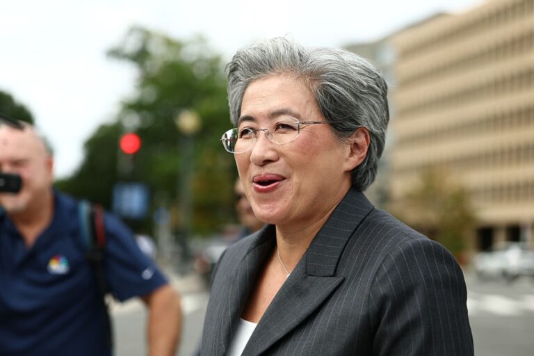
Finn Gomez/Getty Images
AMD Chair and CEO Lisa Su landed in Seoul on Wednesday for her second visit to South Korea in seven months, spending the day in back-to-back meetings with the leaders of Samsung Electronics and SK Hynix — the two companies that collectively control more than 80 percent of global high-bandwidth memory revenue, and whose allocation decisions will determine when, and in what quantities, AMD’s Helios rack-scale AI systems ship. According to AMD’s official announcement, the visit included AMD Gamer Day 2026 at Yongsan Dragon City and a media Q&A session the same afternoon.
The visit is AMD’s most concentrated supply chain diplomacy of 2026, and it is happening at the CEO level — not with procurement teams — because the constraint AMD faces is not silicon. It is memory. Specifically, it is high-bandwidth memory: a category of chip that AMD itself invented, that only three companies in the world manufacture at meaningful scale, and that every single Helios AI rack requires in quantities of 31 terabytes per system. Getting to that number means AMD needs 432 gigabytes of HBM4 per GPU — 50 percent more than the 288 GB found in Nvidia’s competing Vera Rubin GPU — and 72 such GPUs per rack, making HBM supply the most consequential variable in AMD’s ability to deliver on its data center commitments.
Su met with Jun Young-hyun, Vice Chairman and CEO of Samsung’s Device Solutions division, in Samsung’s Seocho office in Gangnam, and separately with SK Hynix CEO Kwak Noh-jung — meetings that continue the roadmap discussions opened by the March MOU and push them toward the three-to-five-year planning horizons Su has described publicly. “We have gotten great support from both Samsung and SK Hynix, and we view the partnerships on HBM not just one generation but really multiple generations,” Su told reporters at a media briefing in Seoul on Wednesday, citing planning horizons of three to five years or more. “To build a solid supply chain over the long term, it is important to work closely with our partners.”
What High-Bandwidth Memory Is, and Why It Made Seoul Indispensable
High-bandwidth memory did not arrive from a Korean laboratory. It was conceived at AMD in 2008, developed by a team led by AMD Senior Fellow Bryan Black, and brought to JEDEC standardization in 2013 through a proposal co-submitted by AMD and SK Hynix. The first HBM chip was manufactured by SK Hynix; the first product to ship with it was the AMD Radeon R9 Fury X GPU in 2015 — a history detailed in the Wikipedia HBM article. The technology solved a problem that was choking GPU performance: conventional memory interfaces were too narrow to feed chips with the compute throughput AI and graphics workloads demand.
The solution was architectural. Where conventional DRAM connects to a processor over a narrow bus — GDDR6 uses 32-bit channels — HBM stacks multiple DRAM dies vertically and connects them to the GPU through a silicon interposer using through-silicon vias (TSVs) and microbumps, creating a bus up to 2,048 bits wide in the current HBM4 generation. That wide interface means the memory can run at more moderate clock speeds while still delivering bandwidth that dwarfs what conventional DRAM can provide. The MI455X carries 12 HBM4 stacks of 36 GB each, connected over that 2,048-bit interface, producing 23.3 terabytes per second of peak memory bandwidth per GPU. For comparison, HBM3E — the prior generation now shipping in AMD’s MI350X and MI355X — uses a 1,024-bit interface and delivers roughly half that bandwidth per stack.
The manufacturing process for HBM stacks requires extraordinary precision. DRAM dies are thinned to roughly 30 micrometers — about a third the width of a human hair — stacked up to 16 layers high, and interconnected through TSVs. The finished stack then bonds to a silicon interposer fabricated by TSMC under its CoWoS-L (Chip-on-Wafer-on-Substrate, Local interconnect) process. That interposer routes signals between the HBM stacks and the GPU compute dies on the same package. The practical consequence is that HBM4 supply involves two separate chokepoints: the Korean companies that produce the memory stacks themselves, and TSMC’s advanced packaging capacity that assembles them with the GPU. Su’s Seoul visit addresses the first of those chokepoints directly.
Because the DRAM stacking process requires specialized fabrication equipment and yields that have taken years to develop, high-volume HBM manufacturing remains concentrated in three companies — Samsung Electronics, SK Hynix, and Micron Technology — with Samsung and SK Hynix together accounting for the large majority of global output. AMD, the company that proposed the HBM standard and shipped the first HBM product, does not manufacture memory. It designs accelerators and depends entirely on partners to supply the chip at the heart of its most important product line.
What the March MOU Established, and What Wednesday’s Meetings Extended
Su’s first Korea visit, in March 2026, produced the most consequential supply agreement in AMD’s recent history. On March 18, she signed a memorandum of understanding with Jun Young-hyun at Samsung’s advanced manufacturing campus in Pyeongtaek, about 60 kilometers (37 miles) south of Seoul. The Samsung-AMD HBM4 agreement formalized Samsung as AMD’s primary HBM4 supplier for the Instinct MI455X — the first time Samsung had been elevated to primary HBM supplier status for an AMD GPU — and extended collaboration to DDR5 memory for AMD’s 6th Generation EPYC “Venice” server processors. That evening, Samsung Chairman Lee Jae-yong hosted Su for dinner at Seungjiwon, the Samsung Group’s historic guesthouse, where the two executives discussed deepening the partnership across multiple semiconductor categories including, potentially, foundry services.
The March agreement was urgent in part because of competitive dynamics that had already squeezed AMD’s HBM4 access. SK Hynix, which commands approximately 54 to 58 percent of global HBM revenue, had already committed the large majority of its 2026 HBM4 capacity — estimates put the figure at roughly 70 percent — to Nvidia for the Vera Rubin platform. That concentration left AMD with limited access to SK Hynix supply for next-generation products and drove the strategic pivot toward Samsung as the primary memory anchor. With Samsung’s HBM4 achieving what the company described as an “80 percent golden yield” by mid-2026 and the company’s share of HBM4 shipments rising as SK Hynix encountered validation delays in Q2 2026, the March MOU has taken on additional strategic weight.
Wednesday’s meetings represent a continuation of the roadmap work that the March MOU opened. Su has described these conversations in terms that go well beyond any individual purchase order, citing planning horizons of three to five years or more and positioning both companies as co-suppliers rather than alternatives — a supply chain strategy that reduces AMD’s exposure to single-source risk on the memory that now defines its most important product line.
What Is Riding on Helios
The urgency of Su’s second Korea visit in seven months becomes concrete when measured against what AMD has committed to deliver. At the Advancing AI 2026 conference in San Francisco in July, AMD formally launched the Helios rack-scale platform alongside the Instinct MI455X accelerator. A Helios rack integrates 72 MI455X GPUs with 18 6th-generation EPYC Venice processors, per AMD’s Helios rack specifications, along with AMD’s Pensando networking hardware, and a liquid cooling infrastructure, all unified through a 31 TB pool of shared HBM4 memory connected via AMD’s UALink (Ultra Accelerator Link) scale-up fabric — an open alternative to Nvidia’s proprietary NVLink interconnect. AMD has claimed the system outperforms Nvidia’s Vera Rubin NVL72 by 15 percent on FP4 compute performance, with 50 percent greater memory capacity and scale-out bandwidth; those claims, based on AMD’s internal benchmarks, have not been independently replicated by neutral parties as of October 2026.
Su made the memory dependency explicit at the July launch. “Help from SK Hynix and Samsung Electronics is what made the next-generation MI455 and Helios possible as we developed them,” she said. That acknowledgment is not a courtesy; it is an operational reality. AMD’s September 2026 appearance at Citi’s Global TMT Conference produced a candid acknowledgment that the company is actively managing supply constraints: “We need to expand supply, but the supply of components such as HBM and semiconductor substrates is very tight, and there are also constraints on advanced packaging capacity,” an AMD executive stated at the event, per Korea Herald reporting. That packaging constraint refers to TSMC’s CoWoS-L capacity, which serves as the second supply chain bottleneck independent of how much HBM4 Samsung and SK Hynix can produce.
At AMD’s second-quarter 2026 earnings report in August, the company posted data center revenue of $6.7 billion — up 107 percent year over year and representing 58 percent of AMD’s record $11.5 billion in total revenue. CFO Jean Hu stated that data center sales were expected to “accelerate in the second half of 2026, driving stronger overall revenue growth and continued earnings expansion,” with Helios ramp cited as a key driver.
The SK Hynix Question
While Samsung is AMD’s confirmed primary HBM4 partner, Wednesday’s meeting between Su and Kwak Noh-jung carries its own strategic weight. SK Hynix has been so deeply integrated into Nvidia’s supply chain that AMD’s relationship with the company on cutting-edge HBM has been structurally limited. Analysts and Korean trade publications have been watching to see whether AMD and SK Hynix will move toward a more substantive HBM4 arrangement, particularly as demand from AMD, Google, Microsoft, Oracle, and other hyperscalers pushes total HBM requirements well beyond what Nvidia alone can absorb.
Su’s position on this is deliberately balanced. “Samsung, SK Hynix are great partners of ours and very key for us to accomplish our broad ambition in data center,” she said at Wednesday’s briefing, naming both explicitly and noting Samsung’s existing role across DDR4, DDR5, and HBM. The framing positions both companies as co-suppliers rather than alternatives — a supply chain strategy that reduces AMD’s exposure to single-source risk on the memory that now defines its most important product line.
According to AMD’s own assessment, the company serves 8 of the 10 largest AI companies in the world with Instinct GPUs in some capacity, a claim AMD has not independently substantiated with named customers or verified shipment data. Named customer commitments in the public record include a multi-year, multi-gigawatt agreement with Meta and GPU deployments at OpenAI, Microsoft Azure, and Oracle Cloud — all announced across 2025 and 2026. Fulfilling those commitments at scale requires a memory supply chain that is not merely adequate for one product generation but locked in for three to five years of roadmap execution, which is precisely the timeframe Su cited in Seoul on Wednesday.
Why Lisa Su’s Washington Role Makes Seoul Matter More
Su’s supply chain diplomacy is not separate from her technology policy role; the two are extensions of the same strategic problem. In her May 2025 Senate Commerce testimony, Su told lawmakers that the United States needed to build “a robust domestic supply chain for advanced semiconductor manufacturing and packaging,” describing the vulnerability of relying on overseas partners for critical components. She simultaneously serves on the Presidential Council of Advisors on Science and Technology — appointed by President Biden and reappointed by President Trump in March 2026 — alongside Nvidia CEO Jensen Huang, Meta’s Mark Zuckerberg, and other technology executives, and she chairs the Semiconductor Industry Association board.
AMD has spent $8.72 million lobbying the federal government on semiconductor manufacturing and artificial intelligence since the start of 2025. The irony embedded in Wednesday’s meetings is precisely the vulnerability Su identified to Congress: a company powerful enough to testify before the Senate on semiconductor policy, and influential enough to advise two successive presidents, is still dependent on the results of face-to-face meetings in Seoul to determine when its flagship AI product ships at scale. HBM supply is not a procurement detail. It is the physical expression of a strategic gap that Su has been arguing Washington should help close — and that she is, in the interim, closing one bilateral conversation at a time.
On Thursday, Su is expected to attend a Seoul roundtable — confirmed by Korea Times reporting — with the CEOs of Rebellions, FuriosaAI, and Mobilint — and a meeting with Science Minister Bae Kyung-hoon, broadening the Korea visit beyond memory supply into sovereign AI infrastructure and Korea’s ambitions for its own AI semiconductor ecosystem.
Wednesday’s meetings with Samsung and SK Hynix produced no announced agreements. But the conversations they continue — on HBM supply roadmaps extending three to five years, on foundry potential, on multi-generational memory partnerships — will shape the architecture of AI infrastructure long after the individual accelerator models being discussed today are superseded. The chip AMD invented to solve its bandwidth problem has become the chip that determines whether its biggest product can ship.
Frequently Asked Questions
Why does AMD’s CEO need to visit Korea twice in one year just to secure memory supply?
High-bandwidth memory is manufactured at meaningful scale by only three companies globally — Samsung, SK Hynix, and Micron — and Samsung and SK Hynix together control the large majority of global HBM output. AMD’s flagship Helios AI rack requires 31 terabytes of HBM4 per system, with 432 gigabytes per GPU across 72 accelerators. Because HBM supply is already strained — SK Hynix has committed roughly 70 percent of its 2026 HBM4 capacity to Nvidia — securing multi-year supply at the scale AMD needs for its Helios commitments requires CEO-level engagement, not routine procurement.
What technically makes HBM4 different from the previous HBM3E generation — and why does that difference matter for AI?
HBM4’s defining change is a doubling of its memory bus width from 1,024 bits per stack (HBM3E) to 2,048 bits per stack, while adding support for 16-layer die stacking compared to HBM3E’s 12-layer configurations. That architectural change, standardized by JEDEC in April 2025, allows each stack to deliver up to 2 terabytes per second of theoretical bandwidth while also increasing per-stack capacity to up to 64 gigabytes. For large language model inference — which requires moving enormous parameter sets between memory and compute during each token generation — higher bandwidth directly translates to faster, cheaper inference at scale. The MI455X’s total bandwidth of 23.3 TB/s across 12 HBM4 stacks is the specific technical capability that AMD is positioning against Nvidia’s Vera Rubin platform.
What is the connection between AMD’s technology policy positions and these Korean supply chain meetings?
AMD CEO Lisa Su testified before the Senate Commerce Committee in May 2025 that the United States needed a more resilient domestic supply chain for semiconductor manufacturing and packaging — noting that critical components like HBM are manufactured primarily overseas. She is a member of the Presidential Council of Advisors on Science and Technology under both the Biden and Trump administrations, and she chairs the Semiconductor Industry Association. Wednesday’s Seoul meetings represent the practical reality that policy advocacy has not yet produced domestic HBM manufacturing capacity: AMD still depends on Korean partners for the memory at the core of its AI hardware lineup, making Seoul an essential destination for supply chain diplomacy that no domestic alternative currently replaces.
What is UALink, and how does it enable Helios to scale to 72 GPUs in a single rack?
Ultra Accelerator Link (UALink) is AMD’s open-standard scale-up interconnect, designed as an alternative to Nvidia’s proprietary NVLink for connecting multiple GPUs within a rack or pod. In a Helios deployment, UALink enables 72 MI455X GPUs to form a unified accelerator domain that shares the rack’s 31 TB HBM4 memory pool, tunneled over Ethernet. Because UALink is an open standard rather than a vendor-controlled proprietary protocol, AMD has positioned it as a foundation for multi-vendor AI infrastructure — a differentiation point for enterprise buyers concerned about lock-in to any single GPU supplier’s interconnect ecosystem.