HomeAuto Intel CTO: EUV Tool Shortage Caps AI Chip Supply Growth at Roughly Double
Intel CTO: EUV Tool Shortage Caps AI Chip Supply Growth at Roughly Double
October 24, 2026:
Dwarkesh.com
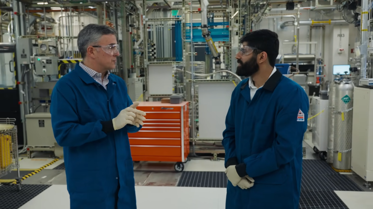
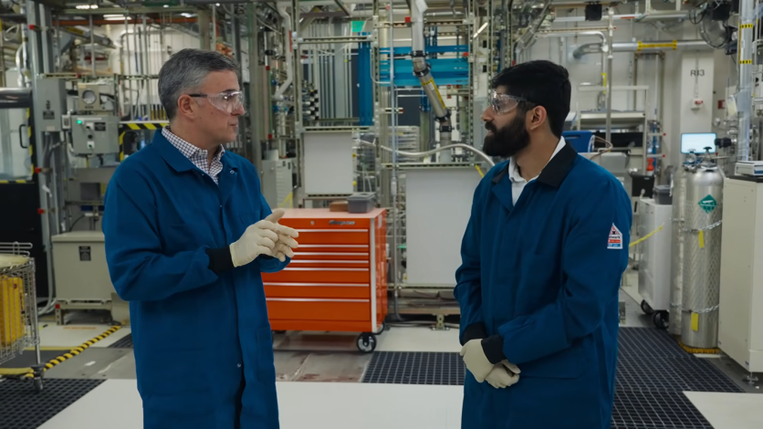
Pushkar Ranade, Intel’s chief technology officer, went on the record this week to explain why every billion-dollar fab announcement in the AI era ultimately collides with the same wall: the world produces fewer than 70 of the machines that make advanced chips, and that number will not change fast enough to matter for AI’s current buildout timeline. Ranade made the remarks in an Intel fab tour podcast published Wednesday on the Dwarkesh Podcast, in a conversation that took Dwarkesh Patel through two days of tours at Intel’s most advanced Oregon fabrication facility.
Speaking on the Dwarkesh Podcast in a conversation published Wednesday, Ranade said that when asked whether the semiconductor industry could expand advanced wafer output by a factor of ten to meet AI’s escalating compute requirements, his answer was unambiguous: no. A doubling is closer to what the industry can realistically achieve, and even that would require a coordination effort across dozens of highly specialized suppliers that has never before been attempted at this pace.
That framing recenters the AI compute debate in a way few executives have been willing to do on the record. The conventional narrative focuses on which company will build the next fab — how quickly TSMC, Samsung, or Intel can pour concrete in Arizona or Ohio. Ranade’s argument is that the constraint is upstream of every fab on earth: it lives inside the toolmakers’ factories in Veldhoven, in the materials chains that feed cleanrooms, and in the specialist workforce that takes years to train. Capital alone cannot fix it.
What Limits the Industry Has Never Built Faster Than
At the center of Ranade’s argument sits ASML, the Dutch company that manufactures every extreme ultraviolet lithography machine used to print the world’s most advanced chips. EUV machines use 13.5-nanometer-wavelength light from a laser-pulsed tin plasma, operate in full vacuum with reflective optics instead of lenses, and weigh nearly 200 tons apiece. Only Zeiss in Germany can manufacture the multilayer mirrors at the optical precision these machines require, and only Oxford Instruments provides the synchrotron light source components. ASML does not make chips; it makes the machine that makes the machines that make the chips.
The 2025 global delivery total: 44 standard EUV systems. ASML confirmed for 2026 a target of roughly 65 Low-NA EUV shipments — up from 44 in 2025, a roughly 50 percent increase year-over-year. ASML’s 2027 guidance calls for at least 80 units. These numbers set the hard outer boundary for how much additional advanced wafer capacity can physically come online.
ASML CEO Christophe Fouquet has said the pressure is real and structural. In a Reuters interview, he said demand for AI is so strong that the market will face constrained supply for quite a long time.
Each new EUV system arrives with an approximately 18-month lead time from order to delivery — meaning today’s order backlog determines the hard ceiling on 2027 advanced-node wafer starts, regardless of urgency or premium pricing. Once delivered, reaching competitive manufacturing yields above 80 percent requires an additional 18 to 24 months of systematic process optimization. That is the compounding lag between a fab announcement and productive chip output.
Why the Constraint Gets Worse, Not Better, With Each Node Shrink
Here is what makes Ranade’s ceiling structurally self-tightening in a way that is not immediately obvious: advanced chips require multiple EUV exposures per layer, and the number of exposures increases with each generation of node shrink.
The underlying physics is the cause. EUV produces stochastic defects — random pattern failures caused by the limited number of photons striking the resist at any given moment — at a rate that grows exponentially as features shrink. Managing this requires either higher dose (which slows throughput) or double and triple patterning (which multiplies the number of EUV machine-hours consumed per finished wafer). The result is that as AI accelerators push to tighter nodes, each chip demands more time on an EUV machine, not the same amount. The effective ceiling on wafer-equivalent AI chip output from the existing EUV fleet is not holding constant — it is declining relative to what the most advanced AI chips require.
This is the deeper layer of Ranade’s argument. The “2× ceiling” he describes applies to the global tool base as a whole. For the specific chips that power frontier AI accelerators — which live on the most advanced process nodes — the practical constraint is tighter still.
Have You Asked Why Building a New Fab Does Not Break This Ceiling?
The logical response to a capacity shortage is more fabs, and the world has committed to exactly that. Amazon, Microsoft, Alphabet, and Meta are collectively on track to spend approximately $725 billion on capital expenditures in 2026, much of it targeting AI infrastructure. GPU and accelerator purchases typically represent 30 to 40 percent of datacenter capital spending, implying chip demand that vastly exceeds what the current ASML delivery schedule can satisfy.
Building a fab does not help if the tools to fill it are backlogged. A leading-edge fabrication facility without EUV machines is a building. The machines arrive on ASML’s schedule, are installed over months, are calibrated over additional months, and yield usable chips only after the process optimization cycle completes. This is why Intel CEO Lip-Bu Tan said in the company’s April 2026 earnings call that “advanced wafer capacity is in short supply” and that global semiconductor supply is not keeping pace with the rapid acceleration in demand — even as Intel was simultaneously ramping one of the world’s largest advanced-node fabs.
An independent analysis of ASML’s Q1 2026 results noted that even with 44 EUV units as the 2025 base, 80 units in 2027 implies EUV wafer capacity roughly doubling relative to 2025 — which is consistent with Ranade’s framing and confirms the 2× ceiling from an external source. The arithmetic does not reach 10×.
Beyond Lithography: The Cascade of Constraints
The cascade does not stop at lithography. Even if ASML could triple its EUV output overnight, the semiconductor ecosystem would immediately collide with the next constraint: cleanroom capacity, process gases, ultra-pure water systems, photomasks, advanced packaging tools, and the trained workforce to operate all of them. Industry data shows that leading-edge logic, DRAM, and advanced packaging are operating at effectively 100 percent utilization, constrained not only by tools but by physical cleanroom floor space. High-bandwidth memory — the stacked chip architecture that feeds AI accelerators — consumes roughly three to four times the wafer area of standard DRAM per unit of memory delivered, compounding pressure on an already stretched wafer supply.
Intel’s Specific Position Inside the Constraint
Ranade’s comments are notable in part because Intel occupies an unusual vantage point: it is simultaneously one of the world’s most ambitious advanced-node fabs and one of the industry’s most significant customers of the tools he is describing.
Ranade holds a PhD in engineering from the University of California, Berkeley, and spent more than 17 years across two tenures at Intel working on transistor process integration — developing the manufacturing techniques for Intel’s 65-nanometer, 45-nanometer, and 22-nanometer process nodes before being named chief technology officer in 2024. He also serves as Chief of Staff to Intel CEO Lip-Bu Tan, placing him at the intersection of Intel’s engineering roadmap and its commercial strategy. His assessment of the EUV ceiling is not theoretical — it reflects direct operational knowledge of how long it takes to ramp a leading-edge fab after the machines arrive.
Intel’s High Numerical Aperture EUV commitment illustrates his point about cost and scarcity simultaneously. The EXE:5200B High-NA EUV machine, which Intel installed in late 2025 for its 14A process node, costs upward of $380 million per system — making it among the most expensive single pieces of manufacturing equipment ever built. Intel and ASML announced in September 2026 that Intel had processed more than one million wafers on High-NA EUV tools to date — more than the rest of the industry combined. ASML CEO Christophe Fouquet, in an official joint press release, described Intel Foundry as “one of the key leaders of the industry’s adoption of High NA.”
Intel also broke ground in July 2026 on a Santa Clara campus expansion specifically designed to produce EUV photomasks for its 18A-P and 14A process nodes. Its Fab 52 in Chandler, Arizona, is designed to support more than 10,000 Intel 18A wafer starts per week at full ramp. Intel has confirmed that volume production on Intel 14A is targeted for the 2028 timeframe.
Every pound of concrete Intel pours in Arizona or Ohio, and every dollar it invests in High-NA EUV, still does not change how quickly ASML can build the machines themselves.
What Policy Can and Cannot Fix
The CHIPS Act and its equivalents in Europe, Japan, and South Korea can fund buildings, equipment deposits, and workforce training. What they cannot do is compress the multi-year sub-supplier ecosystem development that ASML’s own production rate depends on. ASML works with approximately 200 main suppliers and roughly 2,000 companies in its broader supply chain. Expanding any link in that chain takes years of engineering qualification, capital investment, and production ramp — at every sub-tier simultaneously.
One geopolitical dimension is worth noting. Reuters reported in December 2025 that China had secretly completed a prototype EUV machine in Shenzhen, expected to produce working chips between 2028 and 2030. If accurate, this would eventually introduce a second manufacturer to a market ASML currently holds as a monopoly — but “eventually” is doing significant work in that sentence. A prototype and a high-volume manufacturing-capable machine with competitive yield are separated by years of process development that no geopolitical urgency has historically compressed.
The structural conclusion Ranade’s framing points toward is that the AI compute supply challenge is not a question of which company builds the next fab. It is a question of how quickly the entire global semiconductor manufacturing ecosystem can organically scale. On that question, approximately 2× appears to be the honest answer for the near term — and for the most advanced AI chip nodes, the compounding constraint makes even that figure look optimistic.
Frequently Asked Questions
Why can’t semiconductor fabs just build more advanced chips by spending more money?
Building a leading-edge fab requires filling it with EUV lithography machines, and those machines can only be ordered from one company in the world — ASML, based in the Netherlands. ASML shipped 44 EUV systems in 2025 and targets roughly 65 in 2026. Each system takes 12 to 18 months to deliver after ordering, costs between $200 million and $400 million, and requires another 18 to 24 months of process calibration before producing chips at competitive yields. A fab without EUV machines is a building. Capital can build buildings; it cannot accelerate ASML’s sub-supplier ecosystem, which involves approximately 2,000 companies and decades of accumulated engineering.
What is High-NA EUV and why does it matter for AI chip supply?
High Numerical Aperture EUV (High-NA EUV) is ASML’s next-generation lithography platform, capable of printing features at finer pitches than current standard EUV machines. The flagship system, the TWINSCAN EXE:5200B, costs approximately $380 million per unit and runs at 175 wafers per hour. Intel installed one in late 2025 for its 14A process node and has processed more than one million wafers on High-NA EUV tools to date — more than the rest of the industry combined. For AI chip supply, High-NA EUV matters because it enables the next generation of AI accelerator manufacturing — but mass shipments are not expected until 2028 or later, meaning near-term supply depends entirely on the existing standard EUV fleet.
Why does each generation of AI chip require more from ASML’s machines, not the same amount?
Advanced chip manufacturing uses EUV light to print patterns on silicon. As those patterns shrink to improve chip performance, the photon physics of EUV creates a fundamental problem: random variations in where individual photons land produce random defects in the printed pattern — a phenomenon called stochastic defectivity. Managing these defects at tighter pitches requires either exposing the wafer to more EUV light (which slows throughput) or running multiple separate EUV exposures per layer (which multiplies the total machine time per chip). This means the effective chip output from a fixed number of EUV machines decreases as AI accelerators push to finer process nodes, making the supply ceiling tighter than a simple count of machines would suggest.
Will AI chip supply constraints ease by 2028?
Industry executives and analysts have consistently pointed to 2027 and 2028 as the period when relief may begin to arrive — from ASML’s expanding delivery schedule (at least 80 standard EUV units in 2027), from Intel’s 14A volume production targeting 2028, and from TSMC’s N2 ramp. Memory manufacturers SK Hynix and Micron have indicated that high-bandwidth memory shortages may persist into 2028 or even 2030. China’s EUV prototype, reported by Reuters in December 2025 as expected to produce working chips between 2028 and 2030, represents a longer-term potential shift in the competitive landscape. For now, the semiconductor industry’s own statements suggest the current supply constraint has at least two more years of meaningful impact on AI compute availability.