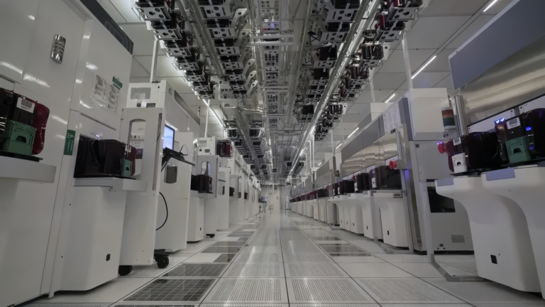
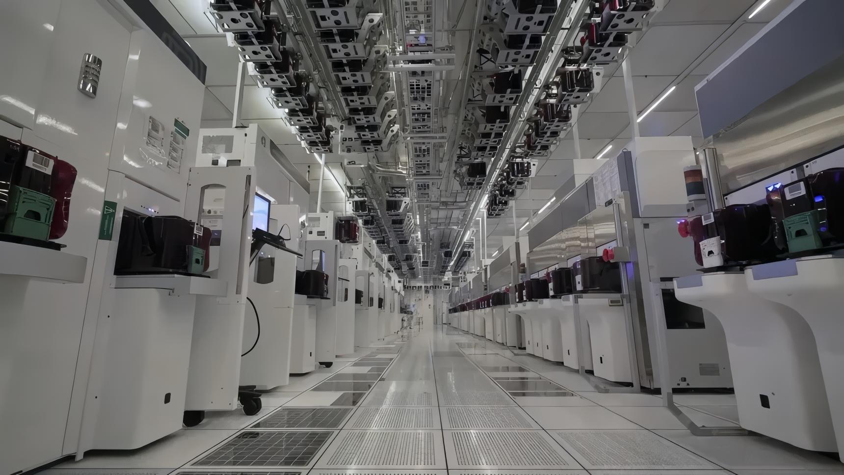
The most important component in an AI chip that most people have never heard of is finally getting a domestic manufacturing address.
GlobalFoundries (GF) announced Wednesday it has signed a $2 billion, five-year manufacturing agreement with TSMC to produce silicon interposers at its Malta, New York fabrication facility — a deal both companies describe as establishing the first US-based supply of this component for TSMC’s CoWoS advanced packaging ecosystem. Volume production is expected to begin ramping in the first half of 2028. The agreement carries an initial five-year term and includes a framework for future capacity expansion.
The critical caveat: producing interposers in New York is not the same as completing CoWoS packaging in New York. Interposers are an upstream input to the full CoWoS process — TSMC’s packaging assembly lines, which bond the interposer to logic dies and high-bandwidth memory stacks, remain concentrated in Taiwan until TSMC’s Arizona and Amkor’s Arizona packaging facilities come online around 2028–2029. In other words, the deal closes one gap in the US packaging puzzle without yet closing the bigger one.
What a Silicon Interposer Actually Does
Understanding why this deal matters requires understanding the component at its center.
Modern AI accelerators — Nvidia’s Blackwell architecture, AMD’s MI-series, Google’s TPUs — are not single chips. They are several dies packaged together inside a single assembly. The logic processor (GPU or AI accelerator) and several stacks of high-bandwidth memory (HBM) sit side by side, connected by a dense highway of fine copper wiring etched into a thin wafer of silicon. That wafer is the silicon interposer.
In TSMC’s CoWoS-S architecture (the variant this deal primarily serves), the interposer sits between the compute dies above and the package substrate below. It contains thousands of through-silicon vias (TSVs) — vertical copper-filled channels drilled through the silicon’s full thickness — that carry signals and power downward to the substrate, and redistribution layers (RDLs) on the interposer’s surface that route signals laterally between the GPU die and the HBM stacks. The density of those lateral connections is what allows HBM to transfer data to the logic die at terabytes per second — a bandwidth impossible to achieve with any off-package connection. Full details of this architecture are documented at WikiChip.
The GF agreement also specifically references embedded deep trench capacitor (DTC) components. DTCs are capacitors formed inside the silicon bulk of the interposer itself using deep trench etching — they provide on-interposer power decoupling, suppressing the voltage fluctuations that arise when a GPU suddenly draws large current spikes. As AI accelerators grow more power-hungry with each generation, managing power integrity at the interposer level has become a meaningful engineering constraint in its own right.
Because interposers require front-end semiconductor processes — the same photolithography, copper damascene wiring, and deep trench etching used to make transistors — they are manufactured at foundries, not at back-end assembly and test houses (OSATs). This is why GlobalFoundries, a foundry with advanced fab processes at Malta, is the appropriate partner for this role rather than an OSAT like Amkor or ASE.
Why CoWoS Has Been a Binding Constraint
TSMC controls an estimated 90% of CoWoS-compatible advanced packaging capacity at AI-chip scale, and that capacity has been operating under severe demand pressure for the better part of three years. By late 2026, TSMC is targeting approximately 130,000 CoWoS wafer starts per month, up from roughly 60,000 in early 2025 — an aggressive ramp — yet analysts estimate the supply-demand gap remains around 20% even at that expanded scale.
The consequences are not abstract. TSMC’s CEO C.C. Wei has publicly stated that CoWoS capacity has been sold out through 2026, according to industry reporting of TSMC’s earnings calls. Nvidia holds approximately 60% of TSMC’s available CoWoS allocation, per Morgan Stanley analysis cited across multiple industry publications. Google reportedly cut its 2026 Tensor Processing Unit (TPU) production target from approximately 4 million to roughly 3 million units — a 25% reduction — directly because of constrained CoWoS access. Intel CEO Lip-Bu Tan noted on the company’s second-quarter 2026 earnings call that customers have been exploring its EMIB-T packaging technology as an alternative to CoWoS precisely because of this capacity problem.
The bottleneck has also created a geographic problem. Chips fabricated at TSMC’s Arizona fabs — built in part to reduce US dependence on Taiwan-based production — are currently shipped back to Taiwan for CoWoS packaging, a supply chain arrangement that critics have characterized as a roughly 12,000-mile round trip that undermines the supply security rationale for domestic wafer fabrication. The distance cited is approximately 19,300 km.
What Makes GF’s Position Unusual Here
GlobalFoundries is not a leading-edge wafer foundry. It does not compete with TSMC at 3nm or below. After exiting the sub-14nm race in 2018, GF repositioned around specialty process nodes — automotive, aerospace, IoT, silicon photonics, and its proprietary FDX (Fully Depleted Silicon-on-Insulator) technology for low-power applications.
Silicon interposers, however, do not require leading-edge transistors. They require sophisticated process capability — fine-pitch copper wiring, precision deep trench etching, TSV formation, yield management across large silicon areas — but not the 3nm or 2nm transistor nodes where TSMC and Samsung compete. GF’s existing Malta fab infrastructure, combined with its US manufacturing footprint and CHIPS Act-backed investments, makes it a technically viable supplier for interposers even without leading-edge process capability.
“Advanced packaging is becoming increasingly critical to delivering the performance, power efficiency and scale required for next-generation AI systems,” said Ed Kaste, GF’s senior vice president of CMOS Business, in the company’s announcement. “By providing manufacturing service using GF’s trusted US manufacturing footprint, we are creating a secure, scalable source of essential advanced-packaging elements that will help customers accelerate innovation and strengthen the semiconductor supply chain.”
The agreement provides a framework for future capacity expansion beyond the initial scope — an acknowledgment that interposer demand is expected to grow with successive CoWoS generations.
It is worth noting that TSMC has not issued an independent statement confirming the deal. The announcement came entirely through GF’s own press release and investor channels; data center infrastructure outlet Data Center Dynamics confirmed the deal through GF’s materials.
What This Closes — and What It Doesn’t
Where Does the US AI Packaging Gap Actually Stand?
Assembling AI chips domestically at scale requires several distinct steps, each of which has its own facility, timeline, and supplier:
Wafer fabrication (leading-edge logic): TSMC Arizona fabs are in production, though currently running primarily at 4nm-class nodes with 2nm targeted for 2026–2027.
Silicon interposer production: PREVIOUSLY: no US-based supplier. AFTER THIS DEAL: GF Malta, targeting first-half 2028.
CoWoS packaging assembly (bonding interposer + logic dies + HBM): TSMC Arizona is building this capability, targeted “before 2029” by TSMC Deputy COO Kevin Zhang in April 2026. Zhang confirmed this timeline in comments to Reuters. Amkor Technology is building a $2 billion advanced packaging and test facility in Peoria, Arizona, backed by $407 million in CHIPS Act funding from the Department of Commerce, targeting early 2028 production.
HBM memory: Dominated by SK Hynix, Samsung, and Micron; no US-based HBM fab is currently operational at AI-chip scale.
The GF-TSMC deal fills in the interposer line — one that no other US investment plan had previously addressed as a standalone supply. But until Amkor Peoria and TSMC Arizona’s packaging lines reach production, interposers made in Malta will still need to travel to Taiwan for CoWoS assembly. The 12,000-mile round trip problem is thus narrowed, not eliminated, before 2028.
Intel Offers a Different Path — with Trade-Offs
Intel’s EMIB (Embedded Multi-die Interconnect Bridge) packaging takes a fundamentally different approach to the problem CoWoS solves: instead of a large monolithic silicon interposer, EMIB embeds smaller silicon bridges only at the die-to-die interface zones within an organic package substrate. This lowers cost and enables larger package footprints, but comes at the price of lower interconnect density across the full die face compared to a full CoWoS-S silicon interposer — and does not easily accommodate the DTC power-integrity features CoWoS-S provides.
Intel’s EMIB-T evolution is designed to allow “designs to be converted from other packaging technologies with minimal redesign,” according to Intel’s own materials, making it a more accessible alternative for customers considering a switch. Google, Meta, and SK Hynix are among the companies reportedly evaluating EMIB-T for select programs. But converting existing Nvidia Blackwell or AMD MI-series designs — optimized for CoWoS-S’s interconnect architecture — to EMIB-T is non-trivial. The most performance-demanding AI training workloads are likely to remain CoWoS-dependent through at least 2028.
GF’s Broader Context: From Specialty Foundry to AI Packaging Partner
The TSMC interposer deal fits within GlobalFoundries’ larger strategic push in 2025–2026 toward becoming a more complete participant in the AI supply chain. In November 2025, GF licensed TSMC’s gallium nitride (GaN) process technology after TSMC announced its exit from GaN foundry services. In June 2025, GF announced a $16 billion investment program spanning its New York and Vermont facilities, including the launch of its New York Advanced Packaging and Photonics Center — the first US-based facility dedicated to silicon photonics packaging. GF’s silicon photonics revenue is expected to roughly double in 2026, with management projecting it could exceed $1 billion annually by 2028.
The interposer deal extends GF’s reach into a segment it had not previously participated in at commercial scale for CoWoS — and does so through a collaborative arrangement with a company that, until recently, it has primarily regarded as a competitor.
Frequently Asked Questions
What is a silicon interposer, and why does it matter for AI chips?
A silicon interposer is a thin wafer of silicon that serves as the interconnect platform inside an advanced chip package. In AI accelerators that use CoWoS packaging, the interposer sits between the logic processor (a GPU or AI accelerator die) and stacks of high-bandwidth memory (HBM), providing the dense copper wiring and vertical through-silicon vias (TSVs) that allow data to move between them at terabytes per second. Without the interposer, the memory bandwidth that AI training and inference systems require cannot be delivered. Every major AI accelerator using HBM — including Nvidia’s Blackwell-generation GPUs and AMD’s MI-series — depends on this component.
Does the GF-TSMC deal mean AI chips can now be manufactured entirely in the United States?
Not yet. The deal creates a US-based supply of silicon interposers — one upstream component of the AI chip supply chain that previously had no domestic source. But the full CoWoS packaging process (bonding the interposer, logic dies, and HBM together into a finished accelerator) still takes place in Taiwan until at least 2028, when Amkor Technology’s Peoria, Arizona facility targets production and TSMC’s Arizona packaging line is expected to come online. HBM memory also has no US-based manufacturing at AI-chip scale. The deal is meaningful progress toward a complete domestic supply chain — not its completion.
What is the difference between CoWoS and Intel’s EMIB packaging, and why does it matter?
CoWoS-S uses a large monolithic silicon interposer — a full wafer of silicon with wiring on its surface and through-silicon channels through its body — to connect dies and memory. Intel’s EMIB (Embedded Multi-die Interconnect Bridge) uses small silicon bridges embedded only at the die-to-die connection points in an organic substrate, avoiding the cost of a full interposer. EMIB is typically lower cost and supports larger package sizes; CoWoS-S provides higher interconnect density and can integrate deep trench capacitors for power integrity. Most existing Nvidia and AMD AI accelerator designs are optimized for CoWoS, making a switch to EMIB a non-trivial re-design. Both approaches are being actively expanded, and the competitive pressure between them is one reason the industry is moving quickly to diversify CoWoS supply — including through deals like the one GF and TSMC signed this week.
When will the United States have a complete domestic supply chain for AI chip packaging?
The realistic window is 2028–2029. GF Malta targets first-half 2028 for silicon interposer production. Amkor’s Peoria facility targets early 2028 for CoWoS-compatible packaging. TSMC’s Arizona packaging facility targets “before 2029,” per TSMC Deputy COO Kevin Zhang’s April 2026 statement. High-bandwidth memory, the remaining critical component, has no confirmed US manufacturing facility at AI-chip scale. Supply chain analysts generally expect that through at least 2027, US-fabricated wafers will continue to depend on Taiwan for advanced packaging assembly.