November 16, 2026:


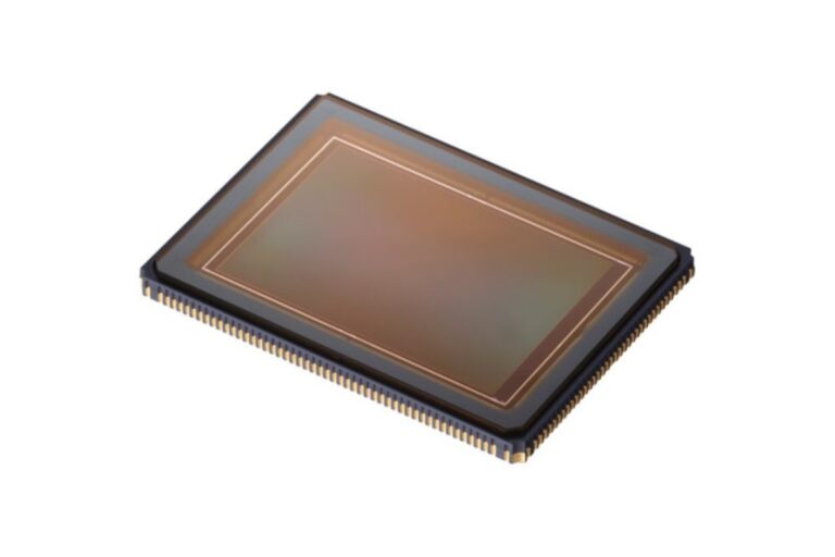
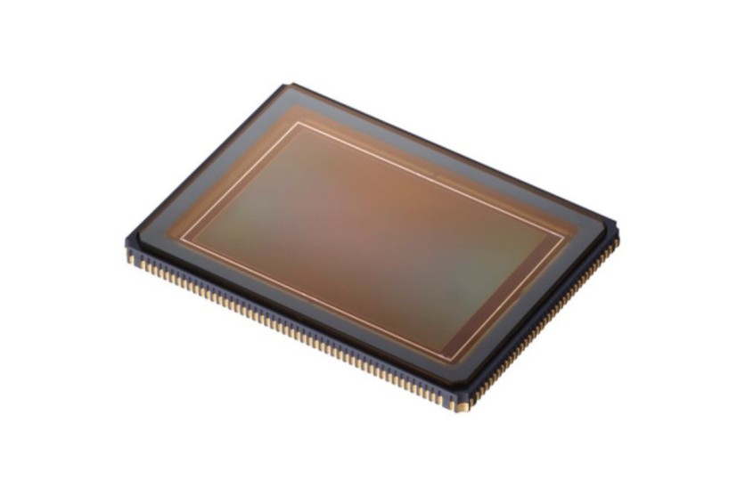
Macnica Americas, the North American division of Yokohama-based Macnica, now says on its product page that engineering samples of Canon’s 410-megapixel LI8030SA sensor are available and that complete evaluation systems are ready to ship, according to a Y.M.Cinema Magazine report published November 14. For chip-inspection engineers it is a signal that they may be able to begin evaluating hardware; for photographers it confirms this is not a camera sensor. TechTimes arithmetic from the published specifications suggests the real limits now sit in the lens and the data link, not on the chip.
Canon has not declared the sensor finished. Canon’s own product page lists the LI8030SA as in development and says its specifications can change without notice. Macnica’s page also says the sensor is in development at Canon, adds that Macnica is scoping early samples and design-in timelines, and invites visitors to join a waitlist. That wording sits awkwardly beside its statement that samples are available, so readers should treat availability as Macnica’s claim, not an independently confirmed shipping status. Y.M.Cinema says mass production has not been confirmed, and no price appears in its report.
Canon announced the sensor on January 22, 2025, calling it the highest pixel count ever achieved in a 35 mm (1.38 in) full-frame sensor, a claim the release limits to Canon’s own survey as of January 21, 2025. Canon showed it at the Shanghai P&I exhibition in July 2025, when Capture magazine reported that Canon had begun accepting inquiries from interested parties. Macnica’s July 2026 newsletter was already promoting the sensor as one that captures an entire wafer in a single frame, but that newsletter does not mention samples. Macnica’s product page carries no date, so when the sample wording appeared is not established.
Macnica says the sensor is being validated across six application areas, citing Canon’s own target-market analysis. They are wafer and chip production inspection; 2.5D and 3D package inspection of through-silicon vias, redistribution layers and micro bumps down to roughly 25 to 30 microns (0.001 to 0.0012 in); astronomical observation; microbial and bacterial detection; wide-area monitoring and license plate recognition; and simultaneous inspection of multiple objects or full panels.
The pitch is that one very large image avoids stitching many smaller exposures. Macnica’s July newsletter says the sensor can capture an entire wafer in a single frame and reveal defects that conventional cameras miss. Capture magazine floated a similar use: automated inspection of a large area at micron-level detail without stitching lower-resolution images, which it framed as a hypothetical industrial case.
Canon’s January 2025 release named surveillance, medicine and industry as example target markets. Neither that release nor Macnica’s six-item list names cinema, and Y.M.Cinema says the sensor was not designed mainly for filmmaking, citing its 8 frames per second ceiling, rolling shutter and small pixels.
Canon says the sensor uses a back-illuminated stacked structure in which the pixel layer and the signal-processing layer are interlayered, plus redesigned circuitry. In a back-illuminated sensor the wiring sits behind the light-sensing layer so more light reaches it, and stacking moves circuitry behind the pixels, freeing area and allowing faster readout. Canon rates readout of 3,280 megapixels per second at 1.5 µm (about 0.00006 in) pixels.
The data load is the engineering price. The sensor outputs through 16 lanes of SLVS, a high-speed serial data link, at 3.84 Gbps each, 14 bits per pixel. By TechTimes arithmetic, that is 61.4 Gbps of raw lane capacity against about 45.9 Gbps of pixel payload at 3,280 megapixels per second. Each full frame holds about 719 MB of packed 14-bit values, so continuous capture at 8 frames per second means roughly 5.75 GB per second before compression. For context, Capture estimated a 410MP file would run about 225 MB, against 25 MB for a compressed raw file from a 45MP sensor.
Canon’s earlier 250MP LI8020SA, an APS-H sensor with the same 1.5 µm (0.00006 in) pixels, runs at 5 frames per second at full resolution. That is about 1.23 billion pixels per second, so the LI8030SA moves roughly 2.7 times as many pixels per second (TechTimes arithmetic from both sensors’ pixel counts). The sensor draws 4.8 W typical at full-resolution readout at 8 frames per second.
The faster mode comes with a catch. The monochrome LI8030SAM can bin four adjacent pixels into one to reach 24 frames per second at about 100 megapixels, a mode Canon’s release restricts to monochrome, so the color LI8030SAC does not get it. Binning merges neighboring pixels, trading fine detail for sensitivity and, on some sensors, speed. The sensor also uses a rolling shutter with progressive scan. Rolling shutters expose rows at different times, which can skew a moving subject or camera. That suits a wafer on a stage better than a moving scene, in TechTimes’ reading.
The figures below come from Canon’s sensor page and Macnica’s listing, and carry the subject-to-change caveat.
| Parameter | LI8030SA |
|---|---|
|
Effective pixels |
24,592 × 16,704 (about 410 MP) |
|
Sensor size |
Full frame, 44.6 mm (1.76 in) diagonal |
|
Pixel size |
1.5 µm (about 0.00006 in) square |
|
Architecture |
Back-illuminated, stacked CMOS |
|
Shutter |
Rolling, progressive scan |
|
Frame rate |
8 fps at full resolution; 24 fps at about 100 MP with 4-pixel binning (monochrome only) |
|
Readout speed |
3,280 megapixels per second |
|
Output |
16-lane SLVS, 3.84 Gbps per lane, 14-bit |
|
Power |
4.8 W typical at 8 fps full readout |
|
Saturation / dark noise |
3,900 e⁻ typical / 4.0 e⁻ rms typical at 6 dB gain |
|
Package |
Ceramic LCC 170-pin plus LGA 316-pin, 51.24 × 37.42 × 3.72 mm (2.02 × 1.47 × 0.15 in) |
The family comes in two versions, the LI8030SAC (color) and LI8030SAM (monochrome). Canon calls the resolution equivalent to 24K, which is 198 times Full HD and 12 times 8K. Y.M.Cinema rounds the horizontal figure to about 24.6K.
Capture magazine noted in July 2025 that many ordinary lenses likely lack the sharpness to match the sensor’s resolving power. Diffraction explains why. Even a perfect lens spreads a point of light into a small disk, called an Airy disk, whose size depends on wavelength and f-number, not on pixel count. In Wikipedia’s worked example, an f/8 lens with 0.5 µm (0.00002 in) light produces a 9.76 µm (0.0004 in) spot. That spot would cover about six and a half of the sensor’s 1.5 µm (0.00006 in) pixels.
Cambridge in Colour’s diffraction tutorial treats an Airy disk roughly 2 to 3 pixels across as the resolution limit for a perfect lens. Applying the same relationship at 550-nanometer (about 0.000022 in) green light, with a disk diameter of about 2.44 times wavelength times f-number, TechTimes arithmetic puts a 2-pixel disk near f/2.2 and a 3-pixel disk near f/3.4. The practical reading is that the sensor rewards fast, high-quality lenses used near wide open, and that stopping down to gain depth of field costs detail sooner than on a lower-resolution sensor. The 1.5 µm (0.00006 in) pitch also implies a Nyquist limit near 333 line pairs per millimeter (TechTimes arithmetic).
The format claim needs the same care. Canon lists a 44.6 mm (1.76 in) imaging diagonal. From the pixel count and pitch, that works out to an active area of about 36.9 × 25.1 mm (1.45 × 0.99 in), slightly larger than the 35.9 × 23.9 mm (1.41 × 0.94 in) sensor in Sony’s a7 IV. “Works with full-frame lenses” therefore depends on a lens covering that larger image area. Macnica’s page does not say what its evaluation systems contain, such as lens, camera body or compute hardware.
Macnica does not publish the wafer size or the optical setup behind its single-frame claim, so the following is TechTimes arithmetic under stated assumptions. This assumes a 300 mm (11.8 in) wafer, the size that tools such as ZEISS’s NLX-100 inspect. Imaged across the sensor’s 16,704-pixel short side, that gives about 18 µm (0.0007 in) of wafer per pixel, which implies roughly a 12-to-1 optical reduction.
Macnica’s package-inspection line cites features down to roughly 25 to 30 µm (0.001 to 0.0012 in). At 18 µm per pixel, a 25 to 30 µm feature spans only about 1.4 to 1.7 pixels, short of the two pixels, one for the object and one for the space beside it, that a clean sampling rule of thumb calls for. Wikipedia’s Airy disk article makes a related point: pixels smaller than half the spot size add little resolution. Both claims can hold only with a smaller field of view, several captures or a different optical arrangement, and Macnica does not say which applies. That is a gap in the public specification, not evidence that either claim is wrong.
The scale problem is not unique to this sensor. A Semiconductor Engineering report describes the imaging challenge in wafer and package inspection as a very high ratio of scanned area to required measurement resolution, on the order of a billion to one for a 300 mm (11.8 in) wafer. Optical inspection alone is not enough for complex packages, ASE’s Eelco Bergman told Semiconductor Engineering, who named X-ray and acoustic microscopy as established options. A single-frame optical sensor is one layer in that stack, not a replacement for it.
No price appears in Y.M.Cinema’s report, Canon still lists the sensor as in development, and Macnica’s own page leaves the availability wording unresolved. Engineers who want to evaluate the LI8030SA can use Macnica’s waitlist and ask the questions this article could not answer from public pages: the optical setup behind the whole-wafer claim, the contents of the evaluation system, the lens recommendations, and the price. For everyone else, the sensor is a measure of what stacked back-illuminated manufacturing can reach at 1.5 µm (0.00006 in) pixels, and a reminder that a record pixel count shifts the hard problems to lenses, data pipelines and sampling.
Macnica’s page says engineering samples are available and complete evaluation systems are ready to ship, but the same page and Canon’s own page say the sensor is in development with specifications subject to change, and Y.M.Cinema’s report gives no price.
Canon named surveillance, medicine and industry as example target markets. Y.M.Cinema says the sensor was not designed mainly for filmmaking, and PetaPixel wrote in July 2025 that cost would keep it a highly specialized tool. PetaPixel added that the technology behind the sensor could inspire the next generation of commercially viable full-frame Canon sensors.
No. Canon uses 24K as a pixel-count comparison, equal to 198 times Full HD and 12 times 8K. At full resolution the sensor runs at 8 frames per second, and 24 frames per second is available only at about 100 megapixels on the monochrome version using four-pixel binning.
One large frame avoids the seams of stitching many smaller exposures, a use Capture magazine described as hypothetical. The trade is that the lens, the data link and the sampling arithmetic become the limits: about 5.75 GB per second at 8 frames per second, apertures near f/2.2 to f/3.4 to keep detail, and, under the assumptions above, about 18 µm (0.0007 in) of wafer per pixel for a whole 300 mm (11.8 in) wafer (all TechTimes arithmetic).