AI Data Centers Join EVs as SiC Demand Engines in Infineon-Wolfspeed 200mm Wafer Deal

October 19, 2026:

AI Data Centers Join EVs as SiC Demand Engines in Infineon-Wolfspeed 200mm Wafer Deal

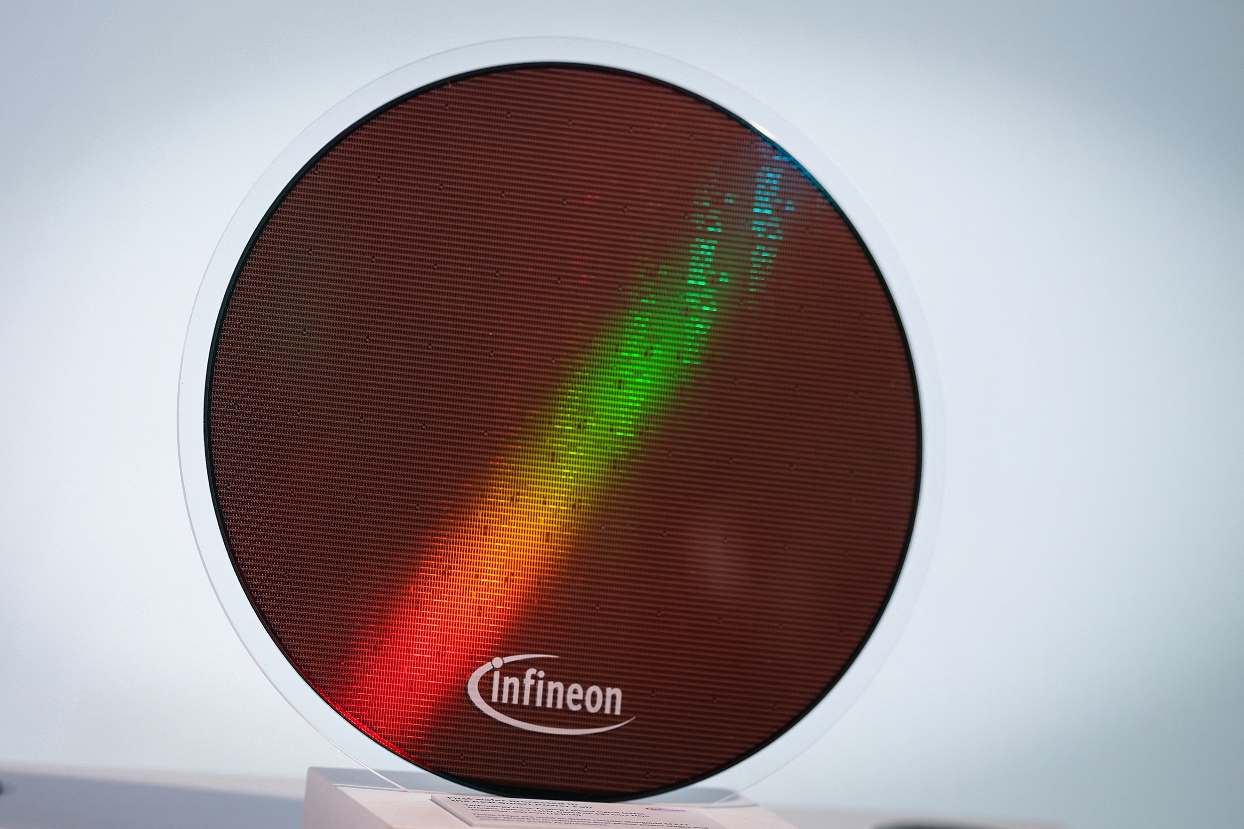
Silicon carbide power chips — the semiconductors that manage energy conversion inside electric vehicles and, as of 2026, inside AI data center power systems — secured a key supply chain commitment on October 15 when Infineon Technologies and Wolfspeed announced a multi-year 200mm wafer supply deal upgrading their 20-year wafer supply relationship from 150mm (~5.91 in) to 200mm (~7.87 in) diameter substrates.

The deal arrived one week after the U.S. Department of War (formerly the Department of Defense; DoW) announced a conditional $1.5 billion loan commitment to Wolfspeed — a pairing that frames this as more than a routine supplier contract: a national-security-backed bet on domestic SiC production at the moment when demand for the material has crossed from electric vehicles into the power infrastructure of artificial intelligence.

Why 200mm Wafers Are the Economic Case for SiC at Scale

The shift from 150mm (~5.91 in) to 200mm (~7.87 in) wafers is the semiconductor industry’s most direct lever for reducing the per-unit cost of silicon carbide chips. A 200mm wafer contains approximately 78 percent more die area per wafer than a 150mm wafer — the area ratio (200²/150²) equals approximately 1.78 — which means more chips can be cut from each substrate and the fixed costs of growing, polishing, and processing that substrate spread across a larger number of finished die.

For silicon carbide specifically, that cost lever is the industry’s primary mechanism for closing the price gap with conventional silicon power devices. Growing bulk SiC crystal by physical vapor transport (PVT) requires temperatures approaching 2,700°C (4,892°F) and yields a material far more prone to defects and growth challenges than silicon. A 200mm wafer does not make those challenges disappear; it spreads their cost across more usable chips.

Alexander Gorski, Infineon’s Chief Operations Officer, described the supply logic plainly. “Silicon carbide is at the heart of the energy transition, and securing a high-quality, resilient supply of 200-millimeter substrates is essential to delivering on our customers’ long-term commitments,” he said in Gorski’s announcement statement. “This agreement further broadens our strong supply base for our 200-millimeter high-volume manufacturing, building on a 20-year supply relationship between our two companies. It strengthens supply chain security for our customers and provides additional flexibility and scalability to support Infineon’s future growth.”

Neither company disclosed the financial terms of the agreement, nor the specific volumes or duration of the contract — standard practice in long-term semiconductor supply deals where pricing is commercially sensitive.

What AI Data Centers Actually Need From SiC Power Chips

The headline demand driver for SiC’s commercial growth has been the electric vehicle, but the material’s addressable market shifted meaningfully between 2024 and 2026. Yole Group’s SiC market forecast projects the market reaching $11 billion by 2031 at approximately 20 percent compound annual growth, driven by EVs, renewable energy, battery storage, and AI data center power infrastructure.

AI data centers have emerged as a distinct demand category with unusual speed. Training and inference clusters operate at power densities and voltage levels that exceed what conventional silicon-based power transistors manage efficiently. Silicon carbide’s wider bandgap — 3.26 electron volts for the 4H polytype versus silicon’s 1.12 eV — gives it a roughly tenfold higher breakdown electric field, allowing it to switch faster and operate at higher temperatures with lower energy losses per switching cycle. Modern AI accelerator racks can draw 30 kilowatts or more of power; those efficiency differences compound across thousands of simultaneous servers in a hyperscale facility, making AI data center SiC demand a structurally distinct market category.

Infineon set a fiscal 2026 AI-related revenue target of €1.5 billion (~$1.73 billion USD; exchange rate as of August 7, 2026, XE.com mid-market; conversions are approximate), with plans to reach €2.5 billion (~$2.89 billion USD) by fiscal 2027. Wolfspeed reported that its AI data center-related revenue roughly doubled over three consecutive quarters in fiscal 2026, even as its automotive segment faced headwinds from soft EV demand.

As Abbas’s market analysis note from Yole compound semiconductor analyst Ahmad Abbas states: “Power SiC is no longer an automotive-only story. The emergence of AI data centers is creating a new demand driver alongside EVs, renewable energy, and energy storage, making the market more diversified and resilient.”

Wolfspeed’s Road From Chapter 11 to Pentagon Backer

Wolfspeed submitted Wolfspeed’s June 2025 bankruptcy filing on June 30, 2025, burdened by the capital demands of scaling 200mm SiC manufacturing capacity faster than customer revenue could absorb. The Durham, North Carolina-based company completed Wolfspeed’s Chapter 11 plan emergence on September 29, 2025, with a restructured balance sheet: debt reduced by approximately $4.6 billion — roughly 70 percent of its pre-bankruptcy obligation — and a new strategic anchor in Renesas Electronics, which took a 16.9 million-share position worth approximately $292 million at emergence, representing approximately 38.7 percent of Wolfspeed’s post-emergence equity.

Robert Feurle, whose background includes senior roles at Micron Technology, Infineon Technologies, and ams-OSRAM, is documented in Wolfspeed’s CEO appointment announcement as having joined as CEO on May 1, 2025. He has since led the company’s push to demonstrate financial stability to investors, customers, and government partners alike.

On October 7, 2026 — one week before the Infineon deal was announced — the U.S. Department of War announced Wolfspeed’s conditional DoW loan: a commitment of up to $1.5 billion to Wolfspeed over 30 years, to be delivered through the department’s Office of Strategic Capital. In exchange, the DoW would receive warrants covering up to 7.5 percent of Wolfspeed’s fully diluted equity. The loan remains subject to due diligence and definitive agreements and requires Wolfspeed to raise $750 million in new equity as a condition of drawdown — it will not be finalized under its current structure unless those conditions are met.

The DoW’s conditional commitment reflects an assessment that domestic SiC production represents a national security priority. Wolfspeed’s Mohawk Valley 200mm SiC fab in upstate New York was the first purpose-built, large-scale 200mm SiC device manufacturing plant in the world, and its North Carolina and Arkansas operations produce the substrate wafers that feed it. A long-term anchor purchase agreement with a customer like Infineon supports the demand-side visibility that justifies maintaining that capacity at scale.

Kulim 3: The Facility This Deal Is Designed to Feed

The Wolfspeed agreement most directly targets Infineon’s Kulim 3 fab opening in Malaysia, inaugurated on August 8, 2024. Designed to become the world’s largest and most competitive 200mm silicon carbide power semiconductor fab, the facility covers 141,640 square meters (~1,524,620 sq ft) and will generate approximately 4,000 jobs, 1,500 of them in high-value technical roles.

Kulim 3 carries an initial capital investment of €2 billion (~$2.31 billion USD) with a further €5 billion (~$5.78 billion USD) in planned expansion, for a total committed investment of €7 billion (~$8.10 billion USD), per Kulim 3 capital investment totals. Infineon’s stated long-term target is to capture approximately 30 percent of a projected €20 billion (~$23.13 billion USD) global SiC market by the end of the decade — implying roughly €7 billion (~$8.10 billion USD) in SiC revenue from the Kulim site alone.

The facility operates under what Infineon calls a “One Virtual Fab” concept, tightly integrated with its power semiconductor competence center in Villach, Austria, which shipped its first 200mm SiC-based products to customers in early 2025. The Wolfspeed supply agreement expands the substrate sourcing for both fabs as the combined 200mm ramp accelerates.

Infineon’s supply relationship with Wolfspeed traces to February 2018, when Wolfspeed operated under the Cree brand name. The two companies extended that arrangement in January 2024 with a 2024 150mm capacity reservation deal; the new agreement replaces that commitment with the upgraded format.

How Does the Section 301 Investigation Into Chinese SiC Affect This Supply Chain?

Infineon maintains a deliberate multi-source substrate strategy — no single supplier controls a critical share of its SiC input. In 2023, Infineon added SICC (Shandong Tianyue Advanced Technology), a Chinese SiC wafer manufacturer listed on the Hong Kong exchange, to its supplier roster.

SICC is subject to China’s National Intelligence Law (2017), Article 7 of which legally requires all Chinese organizations and citizens to “support, assist, and cooperate with national intelligence work,” and to China’s Data Security Law (2021) and Cybersecurity Law (2017), which mandate data localization and government access to data processed on Chinese systems. These obligations attach regardless of where a company’s customers are located or what its contractual privacy representations state.

On December 23, 2024, the US Trade Representative launched USTR’s December 2024 Section 301 probe into Chinese foundational and legacy semiconductor chips, explicitly including SiC substrates. The investigation is designed to examine whether Chinese government subsidies and pricing practices constitute actionable trade violations — and to establish a regulatory basis for tariffs or procurement restrictions that would protect US and Western SiC producers, including Wolfspeed.

The DoW loan commitment to Wolfspeed, the USTR Section 301 investigation, and Infineon’s ongoing relationship with Wolfspeed occupy the same strategic frame: a coordinated effort by US industrial and defense policy to ensure that the supply chain for a nationally critical semiconductor does not depend structurally on a supplier headquartered under Chinese national security law. The Wolfspeed agreement does not eliminate Infineon’s SICC relationship — it adds US-origin supply scale to a portfolio that already includes multiple geographic sources. But if Section 301 results in tariffs or procurement restrictions on Chinese SiC, the Wolfspeed relationship’s relative cost-competitiveness improves — a dynamic both parties can observe as they negotiate future terms.


Frequently Asked Questions

What is silicon carbide and why do AI data centers need it?

Silicon carbide is a wide-bandgap semiconductor with a breakdown electric field roughly ten times higher than silicon’s and significantly better thermal conductivity. These properties allow SiC transistors to switch at higher voltages and frequencies with lower energy losses than conventional silicon-based power devices. AI data center power systems operate at unusually high power densities — modern AI accelerator racks can draw 30 kilowatts or more per rack — and every percentage point of efficiency gain in power conversion compounds across thousands of simultaneous servers. SiC is particularly suited to the power conversion and distribution stages inside hyperscale AI facilities where silicon reaches its practical switching limits, as documented in analyses of SiC power efficiency advantages.

Does the DoW’s $1.5 billion conditional loan guarantee Wolfspeed’s long-term survival?

No. The commitment announced in October 2026 is conditional, not finalized. It requires Wolfspeed to complete due diligence, reach definitive agreements, and raise $750 million in new equity before any funds become available, per the terms outlined in Wolfspeed’s conditional loan requirements. The loan’s 30-year tenor and equity warrant structure reflect the DoW’s interest in maintaining domestic SiC production capacity — not a blank financial backstop. Wolfspeed’s path forward still depends on demonstrating sustained revenue growth and attracting equity investors willing to provide the matching capital the loan conditions require.

What does the 200mm wafer transition mean for the price of SiC chips?

The 200mm format gives manufacturers approximately 78 percent more usable die area per wafer compared with the 150mm format it replaces, spreading the fixed costs of SiC crystal growth — a physically demanding, high-temperature process orders of magnitude more complex than silicon crystal growth — across a larger number of finished chips. The direct result, as fabs ramp to high-volume production at 200mm, is a lower per-chip substrate cost reduction. That cost reduction is the primary mechanism by which the SiC industry expects to close the price premium versus conventional silicon power devices and make SiC economically viable across a broader range of applications beyond premium EVs and industrial equipment.

Source link