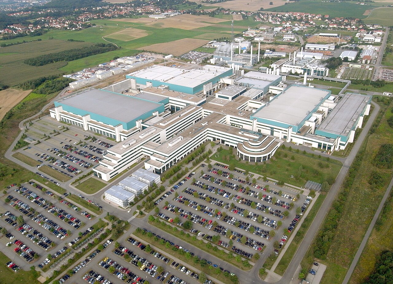
Japan has committed up to $21 billion to build two new semiconductor factories in New York—and will not operate a single one. Instead, GlobalFoundries, the Malta, New York-based contract chipmaker, will manage construction, run daily operations, and license its process technologies to the joint US-Japanese-owned facilities. The arrangement, announced Wednesday under the Trump administration’s newly formalized US-Japan Strategic Investment Initiative, is the first time a foreign allied government has funded large-scale semiconductor manufacturing capacity on US soil for a US company to operate — and the deal’s architects are already calling it a template. The announcement was filed as a US-Japan initiative press release with the Securities and Exchange Commission on October 14, 2026.
Japan Provides Capital; GlobalFoundries Provides Operations
The deal’s structure inverts the usual assumptions about who bears which kind of risk in a fab construction project. Japan supplies all of the investment capital: an approximately ten billion initial investment will accelerate construction of a first new 300-millimeter (12-inch) wafer fab on GlobalFoundries’ existing Malta campus, expected to come online in 2029, with a further roughly $10 billion earmarked for a second fab at the same site. The two factories will be jointly owned by the US government and Japanese interests.
GlobalFoundries, for its part, contributes what it calls differentiated technology, manufacturing expertise, and operational management—and earns fees for each. Under the terms disclosed Wednesday, GF will be paid for construction management, for ongoing factory operations once the fabs are running, and for licensing its process technology to the facilities.
That fee-based structure is significant: GlobalFoundries will generate revenue from these fabs without putting up the roughly $20 billion in capital it would otherwise need to build them. The tradeoff is equally significant: GF will not own these factories. If demand falls, the US-Japan trade relationship shifts, or a successor technology makes the fabs’ process nodes obsolete before the investments are recovered, the governments — not GF — hold the assets.
CEO Tim Breen said the selection validated the company’s operational track record. “GF was selected because fabs of this scale require more than capital. They require differentiated technology, operational excellence and a proven ability to execute. That combination is what positions GF to make this first-of-its-kind initiative a success,” he said.
When fully operational, each fab is projected to deliver 900,000 wafers annually per facility of 300-millimeter capacity — roughly 75,000 wafer starts per month per facility, for a combined addition of approximately 1.8 million wafers annually to domestic chip production. Together, the two fabs are forecast to create 27,000 jobs in Capital Region construction and ecosystem positions and more than 1,000 permanent high-skilled manufacturing jobs in New York’s Capital Region.
What US Tariff Concessions Produced — and Who Picks Projects
The capital for these fabs traces directly to a US-Japan tariff deal framework negotiated between the Trump administration and Tokyo. Under that deal, the United States agreed to lower tariffs on Japanese imports from 25 percent to 15 percent; Japan, in exchange, pledged to invest $550 billion in the US economy. Japan had already announced prior Japan investment tranches totaling more than $100 billion under the broader framework.
The two Malta fabs are the first semiconductor projects named under the initiative, now formally called the US-Japan Strategic Investment Initiative. A notable feature of the mechanism: the Trump White House selects which specific projects receive Japanese funding. That means the federal government is not simply facilitating bilateral investment — it is actively directing which US companies and facilities receive allied-nation capital, a degree of government involvement in industrial location decisions with few American precedents outside wartime manufacturing policy.
Commerce Secretary Howard Lutnick said the administration’s tariff posture delivered the result. “President Trump’s historic U.S.-Japan Trade Deal is delivering another massive manufacturing investment into America. With Japan’s investment funding and GlobalFoundries’ partnership, two large semiconductor chip manufacturing facilities will be built in the U.S., creating thousands of high-paying jobs for American workers.”
A separate but structurally linked benefit flows back to Japan’s own industrial base. GF CEO Breen noted that a substantial share of the Japanese capital investment will return to chipmaking toolmakers — companies such as Tokyo Electron, which dominates portions of the semiconductor equipment supply chain alongside US counterparts. Tokyo Electron CEO Tony Kawai welcomed the initiative, noting that the company has supported GlobalFoundries’ manufacturing operations globally for years and is “pleased to contribute to expanding advanced semiconductor production capacity in the United States.”
Washington Expands Its Equity Stake as CHIPS Dollars Shift Gears
Wednesday’s announcement also formalized a deepening financial relationship between GlobalFoundries and the US government. The Department of Commerce will receive a four percent equity stake in GF as part of the deal — an expansion from the roughly 1 percent stake the government acquired in July 2026 when it awarded GF $300 million in CHIPS Act funding for silicon photonics development.
The government’s move from approximately 1 percent to approximately 4 percent represents a meaningful increase in its financial interest in GF’s commercial success — and, critics of government industrial policy will note, creates a situation in which the entity setting semiconductor policy also holds a direct financial stake in one of the major beneficiaries of that policy.
In parallel, GlobalFoundries agreed to restructure its existing CHIPS Act award. Under the amended agreement, the 955 million CHIPS Act reallocation redirects funding away from conventional fab expansion — the kind of capacity now being funded by Japanese capital — and toward accelerating GF’s investments in silicon photonics, silicon-germanium, and advanced packaging at its Malta and Burlington, Vermont facilities.
GF had previously received up to $1.5 billion from the CHIPS Act under the Biden administration to expand New York operations and modernize its Vermont facility; the reallocation effectively redirects nearly two-thirds of that award toward higher-margin specialty technology platforms. The practical effect: US taxpayer dollars that would have funded the same kind of commodity 300mm capacity Japan is now building instead flow toward the differentiated technologies — silicon photonics for AI data centers, SiGe for high-frequency analog applications — where GF believes its competitive advantage is greatest.
GF has been targeting a $1 billion silicon photonics revenue target exiting 2028 and a $2 billion longer-term target. Its Silicon Photonic Co-Packaged Advanced Light Engine platform, known as SCALE, aims for 400 gigabits-per-second data transfer speeds with a fivefold improvement in energy efficiency compared to current-generation copper interconnects — a specification directly relevant to the power and bandwidth demands of AI data center infrastructure.
Customer Roster: Apple, GM, Renesas, Cirrus Logic All Committed
The announcement named an unusually detailed set of committed customers across automotive, consumer electronics, and industrial markets — a rare public window into the forward demand underpinning a capital commitment of this scale, and a direct answer to the utilization-risk question that hangs over any new fab of this size.
Apple reiterated its long-standing manufacturing partnership with GF. Apple COO Sabih Khan said the company has “partnered with GlobalFoundries to produce essential chips for Apple products right here in the United States, as part of our $600 billion commitment to American investment,” calling GF an inaugural member of Apple’s American Manufacturing Program.
Renesas Electronics, Japan’s largest chipmaker and a dominant supplier to the global automotive industry, positioned the Malta expansion as a direct extension of its production footprint. Renesas CEO Hidetoshi Shibata said the company is “planning around GF’s new capacity in New York” to ensure “stable, long-term supply” of the semiconductors its products require, especially as demand for vehicle electrification, AI, and connectivity accelerates. Renesas’ commitment carries a strategic logic beyond supply diversification: as a Japanese company, Renesas is both a customer of the fabs Japan is funding and a beneficiary of the allied-nation investment model more broadly.
General Motors framed the deal as part of its push into software-defined vehicles and AI-enabled driver assistance. GM President Mark Reuss said the company’s next-generation Super Cruise system and widespread in-vehicle AI deployment require a resilient domestic semiconductor supply chain, noting that GM and GF had already established the first direct automaker-to-foundry supply agreement and that the Malta expansion “marks a decisive step forward for American manufacturing.”
Cirrus Logic CEO John Forsyth, the Austin-based mixed-signal chip specialist whose components appear in Apple devices and consumer audio hardware, said the new fabs give it “access to important domestic manufacturing capability for next-generation mixed-signal products.”
Malta Becomes One of Western Hemisphere’s Largest Chip Campuses
GlobalFoundries’ Malta campus has Fab 8 operational since 2012 — one of the most advanced specialty semiconductor facilities in the United States. The two new fabs would transform the site into one of the largest dedicated semiconductor campuses in the Western Hemisphere. The Malta site is already permitted and described as shovel-ready, allowing GF to accelerate construction by leveraging existing infrastructure. Groundbreaking on the first fab is expected later this year.
Governor Kathy Hochul praised the announcement as validation of the state’s sustained investment in the Capital Region’s semiconductor ecosystem, calling it “a tremendous vote of confidence in New York’s world-class workforce.” The New York Green CHIPS program, the state-level complement to the federal CHIPS Act providing tax incentives, workforce development funding, and environmental compliance support, is expected to continue supporting the regional buildout.
Grant McEwan Fab 8 manager underscored the workforce dimension. “Since 2009, the people of this site have built one of the nation’s most advanced semiconductor manufacturing operations. These two great countries entrusting GF to operate two new fabs is a powerful vote of confidence in our workforce, our technology and New York’s Capital Region.”
Can Allied-Nation Capital Model Scale to Other Trading Partners?
The deal’s architecture — allied-nation capital paired with a US operator, with profit-sharing and government equity stakes structured on both sides — is being watched closely by semiconductor industry observers as a potential model for future bilateral investments. The Semiconductor Industry Association statement, issued alongside the announcement, called the deal “a major win for U.S.-based chip production and a testament to the strength of the U.S.-Japan partnership” and credited both governments for working toward enhanced manufacturing capacity and supply chain resilience.
The announcement comes one week after GF separately disclosed a two billion interposer agreement with TSMC to supply silicon interposers for advanced AI chip packaging at Malta — a deal that further underscores the company’s rapidly expanding role as a hub of the US-led semiconductor supply chain realignment.
Details of the profit and revenue-sharing structure between American and Japanese interests — including the mechanism by which returns shift toward the US side over time — have profit-sharing structure not yet disclosed and are expected to be addressed in further regulatory filings. The fundamental governance question the structure raises — who makes technology investment decisions when the operator earns fees but the owners bear capital risk — will be a central issue for analysts and policymakers evaluating whether the model can be extended to deals with South Korea, Germany, or other trading partners.
Frequently Asked Questions
What does the allied-nation capital model mean for US semiconductor independence?
It means the United States gains new domestic chip manufacturing capacity — 1.8 million 300mm wafers per year combined across both fabs when fully operational — without the US government or GF having to raise $21 billion in additional capital. The tradeoff is that the US government and Japanese interests split ownership of the fabs, meaning future policy decisions about the facilities involve both governments. For strategic supply-chain purposes, the chips are made on US soil by a US operator with a US workforce; for capital-ownership purposes, the picture is more complex. Whether that tradeoff is favorable depends on how durable the US-Japan strategic alignment proves to be over the multi-decade life of the facilities.
If GlobalFoundries earns fees rather than owning these fabs, how does that affect its incentives?
The fee-based operating arrangement means GF’s revenue from these fabs is relatively stable — it earns fees for construction management, operations, and technology licensing regardless of whether the fabs run at 60 percent utilization or 95 percent. That insulates GF from the utilization risk that has historically threatened foundry expansions during demand downturns. However, it also means GF has limited upside from the fabs’ commercial success compared to an ownership model: if the fabs consistently run full and generate strong margins, most of that financial benefit accrues to the US and Japanese government owners rather than to GF’s shareholders. Further regulatory filings are expected to detail the profit-sharing threshold—the level at which returns shift toward the US side.
What is GlobalFoundries making at Malta, and why does that matter for AI?
GlobalFoundries specializes in what the industry calls specialty or differentiated semiconductors — chips that do not require the most advanced transistor nodes but demand specific performance characteristics such as low power, high reliability, mixed-signal capability, or integration with photonics. Its existing Fab 8 manufactures chips for Apple, GM, and defense customers using its FD-SOI (fully depleted silicon-on-insulator) process, which enables dynamic power-performance control without the extreme ultraviolet lithography equipment that cutting-edge AI processors require.
The CHIPS Act reallocation also accelerates GF’s silicon photonics investment, targeting a platform that can move data between AI processors using light instead of copper at 400 gigabits per second with the SCALE platform energy efficiency of five times the energy efficiency of current-generation interconnects — a potentially significant advantage as AI data centers confront energy and bandwidth constraints.
What is the US-Japan Strategic Investment Initiative, and are more semiconductor deals planned?
The US-Japan Strategic Investment Initiative is the formal name for the framework produced by the Trump administration’s trade deal with Tokyo, under which US tariffs on Japanese imports were reduced from 25 percent to 15 percent in exchange for Japan’s pledge to invest $550 billion in the US economy. The US-Japan investment initiative framework gives the Trump White House the role of selecting which specific projects receive Japanese funding; the two GlobalFoundries fabs are the first semiconductor projects announced.
Japan had previously announced two prior tranches of projects totaling more than $100 billion under the broader deal across multiple sectors. Whether additional semiconductor manufacturing deals follow—with GlobalFoundries, Intel, or other US-based foundry operators—will depend on whether the Commerce Department and Japanese government identify further capacity gaps the allied-nation model can address.