HomeAuto Kioxia LD4 Debuts at OCP Summit: BiCS8 CBA Architecture Validates 122.88 TB in E1.L
Kioxia LD4 Debuts at OCP Summit: BiCS8 CBA Architecture Validates 122.88 TB in E1.L
October 10, 2026:
Americas.kioxia.com
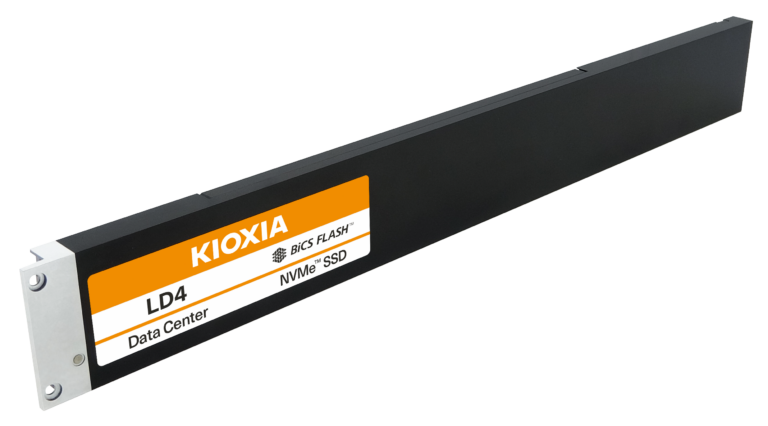
Kioxia announced its LD4 Series on October 8, 2026 — a single-port NVMe SSD in the E1.L “ruler” form factor built on eighth-generation BiCS FLASH QLC NAND, and validated on an architecture the company says supports up to 122.88 TB in a single drive. Drives are sampling now at 15.36 TB and 30.72 TB, with no timeline disclosed for higher-capacity configurations.
The LD4 is scheduled to appear publicly for the first time at the 2026 OCP Global Summit, running October 12–15 at the San Jose Convention Center in California — a sold-out gathering expected to draw 7,000–9,000 hyperscale engineers and procurement teams. For the storage architects at that event, the LD4 represents a direct answer to a specific infrastructure question: how do you pack more read-intensive flash into a 1U chassis without going to a larger, dual-port, PCIe Gen 5 platform?
“The continued growth of data-intensive workloads is driving demand for higher-capacity storage in hyperscale data centers,” said Neville Ichhaporia, senior vice president and general manager of the SSD business unit at KIOXIA America, Inc. “QLC flash is particularly compelling for read-intensive applications, where high capacity and high read performance supports the vast data storage requirements of today’s AI workloads.”
What the E1.L Form Factor Actually Is — and Why It Exists
The E1.L is not a marketing label. It is a standardized physical specification defined under SNIA document SFF-TA-1007, measuring 318.75 mm (12.55 in.) long, 38.4 mm (1.51 in.) wide, and 9.5 mm (0.37 in.) thick — roughly three times the board length of an E1.S “short” drive.
That extended length is the point. A 1U server chassis built for E1.L can accommodate up to 32 drives according to SNIA reference configurations, compared to a handful of 2.5-inch drives in the same vertical footprint. Every additional millimeter of PCB is real estate for NAND packages, and NAND packages are what determine per-drive capacity. The E1.L does not improve read or write speed per drive; it improves terabytes per slot. For object storage, AI inference data lakes, and cold-tier repositories where reads vastly outnumber writes, that distinction maps directly onto rack economics.
The form factor operates on a pure NVMe-over-PCIe interface, hot-pluggable, with 3.3V and 12V power support — advantages that legacy 2.5-inch U.2 drives lack. According to Trendfocus market analysis cited by StorageReview, E1.S currently drives the majority of EDSFF unit volume in hyperscale deployments, but E1.L remains the preferred form factor where capacity density per slot — rather than per-drive performance — is the design constraint.
How BiCS8’s CBA Architecture Enables 4 TB Per Die Package
The capacity the LD4 can reach is a direct consequence of the NAND architecture inside it. Kioxia’s eighth-generation BiCS FLASH introduces a fabrication technique called CBA — CMOS directly Bonded to Array — which represents a structural break from prior 3D NAND manufacturing. That architecture is documented on Kioxia’s BiCS FLASH technology page.
In every prior generation of 3D NAND, the peripheral CMOS circuitry (the page buffers, sense amplifiers, charge pumps, and I/O that service the memory array) was built on the same wafer as the NAND cell array — either next to it (CMOS next to Array, or CnA) or underneath it (CMOS Under Array, or CuA, used by Micron). The problem with both approaches is process coupling: manufacturing NAND cells requires a high-temperature annealing step that can degrade the CMOS transistors if they share the same substrate. Engineers have to find a compromise process that neither the CMOS nor the NAND array is optimized for.
CBA removes that constraint. The NAND cell array and the CMOS logic are each fabricated separately on their own wafers, optimized independently for their respective process requirements, and then bonded together using hybrid wafer bonding technology. The result is a die that Kioxia can push to 218 active NAND layers while delivering NAND I/O speeds above 3.2 Gb/s — a 33% improvement over the seventh generation.
In QLC configuration, a single BiCS8 die holds 1 Tb (1 terabit, or 128 GB) of data by encoding four bits per cell across 16 distinct voltage states. Stack 16 of those dies into a single NAND package and you reach 4 TB per package. Distribute enough packages across E1.L’s 318.75 mm board, and 122.88 TB becomes the architectural ceiling for this generation.
That is not a marketing projection. It is a capacity calculation rooted in die density and board geometry.
QLC NAND’s Engineering Trade-Off — and Why It Fits This Workload
QLC stores more bits per cell than any commercially deployed NAND type, and it pays for that density in write endurance. A standard QLC NAND cell supports approximately 1,000 program/erase (P/E) cycles before reliability degrades — compared to around 3,000 for TLC, 10,000 for MLC, and up to 100,000 for SLC, according to established NAND specifications.
For hyperscale AI storage, that trade-off is acceptable. AI training datasets, inference caches, and object storage repositories are read-dominated workloads. Data is written once, perhaps refreshed infrequently, and then read thousands of times. In this environment, write endurance is not the binding constraint — capacity per watt, capacity per rack unit, and cost per terabyte are.
A standard implementation approach to improving QLC write behavior is SLC caching: the controller temporarily holds incoming data in faster, more durable single-bit-per-cell mode before programming it into QLC cells. SanDisk’s competing UltraQLC platform takes a different approach called Direct Write QLC, which eliminates the SLC buffer and programs data directly to QLC on the first pass, recovering the capacity and power overhead the SLC cache would otherwise consume.
Kioxia has not disclosed which write management strategy the LD4 uses. That is a material detail for operators evaluating write-intensive burst scenarios, checkpointing, or metadata-heavy object storage protocols, and it will need to be confirmed before procurement teams can complete their evaluation.
What the Withheld Performance Specs Mean
Kioxia has not published sequential read or write speeds, random IOPS, read or write latency, power consumption, or drive endurance figures (measured in drive writes per day or total bytes written) for the LD4 Series. That is not unusual for a product in active customer sampling — specifications are typically withheld until they are stable across production silicon — but it means the LD4 cannot be evaluated on performance metrics yet.
What can be inferred: the LD4’s PCIe interface is listed as “PCIe 5.0 specification compliant, up to 16 GT/s across four lanes” — but 16 GT/s per lane is Gen 4 signaling, not Gen 5. As StorageReview’s spec table confirms, a PCIe Gen 4 x4 link caps aggregate sequential bandwidth at approximately 7.9 GB/s in each direction. For a 1U chassis densely populated with 30+ E1.L drives, per-drive bandwidth matters less than aggregate throughput — and the bottleneck in those configurations is more often the network egress or PCIe switch fabric than any individual drive’s interface. Gen 4 is a deliberate positioning choice for infrastructure that runs on Gen 4 PCIe today, which describes the majority of deployed hyperscale hardware.
The LD4’s single-port configuration — as opposed to dual-port designs like Kioxia’s own LC9 — also reflects a deliberate cost and complexity reduction. Dual-port connectivity provides redundant data paths for high-availability deployments requiring transparent failover. Single-port designs are simpler, cheaper, and appropriate for dense scale-out architectures where the cluster itself provides redundancy above the drive level.
How LD4 Fits Into Kioxia’s Portfolio
Kioxia now covers the EDSFF form factor range with three products occupying distinct roles. The NX1 Series, introduced in July 2026, uses the shorter E1.S form factor and includes a liquid-cooled variant — appropriate for thermally challenging dense 1U deployments where E1.S’s lower profile enables tighter packing. The LC9 Series uses the larger E3.L or 2.5-inch form factor with a dual-port PCIe Gen 5 interface and has been validated at up to 245.76 TB — making it the highest-capacity QLC drive Kioxia ships in a dual-path, high-availability configuration. The LD4 fills the space between those two: longer board than E1.S for more capacity, simpler single-port Gen 4 interface than the LC9 for more economical scale-out deployments.
SanDisk’s UltraQLC platform ships a 256 TB drive in U.2 form factor, which surpasses Kioxia’s LC9 in raw capacity. SK Hynix has delivered 122 TB QLC SSDs in the enterprise market and has a 244 TB model on its roadmap. Micron’s 6600 ION reaches 245 TB in E3.L. The enterprise QLC drive market has moved quickly; by mid-2026, eight vendors had announced SSDs at or near the 245 TB mark. In that context, the LD4’s 30.72 TB sampling SKU and 122.88 TB architecture ceiling are positioned not at the capacity frontier but at the 1U density frontier — a narrower and more specific claim.
A Roadmap Beyond 122.88 TB
The 122.88 TB ceiling the LD4 has validated is a function of BiCS8 QLC’s 1 Tb die. Kioxia has announced its tenth-generation BiCS FLASH on a 332-layer architecture with a 2 Tb die — double the per-die capacity of BiCS8 — and a NAND I/O speed of 4.8 Gb/s, itself 33% faster than BiCS8. A future E1.L drive built on BiCS10 QLC would, applying the same package-stacking math, carry a substantially higher capacity ceiling than 122.88 TB — without changing the E1.L slot or chassis.
Kioxia has not announced a BiCS10-based E1.L product. But the architectural trajectory is visible: CBA-based 3D NAND roadmaps consistently increase die density each generation, and the E1.L’s board geometry does not change between generations. That combination is what makes 122.88 TB a waypoint rather than a limit.
OCP Global Summit and What Comes Next
The LD4 is set to make its live demonstration debut at the OCP Global Summit, which opens in San Jose on October 12. The event, which has sold out its capacity of 7,000–9,000 attendees, is where hyperscale engineers from Meta, Microsoft, and major cloud operators converge to evaluate hardware against OCP reference specifications.
The LD4’s partial OCP Datacenter NVMe SSD Specification 2.6 compliance is worth noting: Kioxia states the drive does not meet every requirement of that specification. Which specific requirements fall short has not been published. For operators building tightly OCP-compliant storage stacks, this matters — the OCP specification governs manageability interfaces, telemetry, firmware update protocols, and device health reporting, and any gap in compliance affects interoperability with OCP-validated management toolchains.
Beyond the summit, what the industry will watch for is the performance specification release. Endurance ratings, sequential read and write speeds, and power figures are the inputs to the TCO models that drive hyperscale procurement. Without those numbers, the LD4 is an architectural announcement — a demonstration that 122.88 TB in E1.L is physically possible via BiCS8 CBA QLC, and that Kioxia has a drive in customer hands today at 30.72 TB to prove it. The business case arrives when the specs do.
According to Mordor Intelligence’s January 2026 analysis, EDSFF modules are forecast to grow at an 18.12% compound annual growth rate through 2031 — the fastest among all SSD form factors — and the overall SSD market is projected to expand from $31.31 billion in 2025 to $76.41 billion by 2031. The structural driver is AI infrastructure investment, and the specific product form it takes in dense 1U chassis is exactly the LD4’s proposed role.
Frequently Asked Questions
What does “BiCS8 CBA architecture” mean, and why does it matter for the LD4’s 122.88 TB claim?
BiCS8 is Kioxia’s eighth-generation 3D NAND technology, using 218 active layers and a fabrication method called CMOS directly Bonded to Array (CBA). CBA manufactures the NAND cell array and the CMOS control circuitry on separate wafers — each optimized for its own process requirements — then bonds them together. The result is a denser die (1 Tb per die in QLC configuration) with faster I/O than earlier architectures that integrated both on the same substrate. Stack 16 of those dies in one NAND package, and you reach 4 TB per package. Spread enough packages across the LD4’s 318.75 mm board, and the 122.88 TB ceiling follows from the die density and board area combined. The claim is not speculative — it is the direct consequence of the architecture’s per-die capacity.
What is the difference between the E1.L form factor and the other drives Kioxia sells?
The E1.L (defined under SNIA spec SFF-TA-1007) measures 318.75 mm long — roughly three times the length of an E1.S drive. That extra board length exists purely to carry more NAND packages, which is why E1.L is the preferred form factor when terabytes per 1U slot matter more than per-drive performance. Kioxia’s NX1 uses E1.S (shorter, liquid-cooled variant); the LC9 uses the larger E3.L or 2.5-inch form factor with a dual-port PCIe Gen 5 interface for high-availability, high-performance use cases. The LD4 in E1.L occupies the niche where read-intensive, dense, single-port 1U storage is the design target.
Why hasn’t Kioxia published the LD4’s read speeds, write speeds, or endurance ratings?
Withholding performance specifications during early customer sampling is standard practice in enterprise flash. The figures are typically held until they are stable across production silicon and confirmed under the customer’s qualification testing. What the absence of specs signals is that the LD4 is in the validation stage, not commercial readiness — Kioxia is collecting real-world data from select hyperscale customers before committing to public performance claims. Expect endurance (DWPD or TBW), sequential read/write throughput, and power envelope figures to follow as the qualification cycle advances.
Is 122.88 TB the highest-capacity SSD that will ever fit in an E1.L slot?
Not necessarily. Kioxia’s BiCS10 NAND — announced with a 332-layer architecture and 2 Tb per die, double the BiCS8 die capacity — would, in the same package-stacking configuration, double the capacity ceiling in an E1.L slot relative to BiCS8. The E1.L form factor itself does not change between NAND generations. The 122.88 TB ceiling is an architecture-generation limit, not a hard physical limit of the slot.