HomeAuto AMD EPYC Verano Trades Server Upgradeability for Record Memory Bandwidth
AMD EPYC Verano Trades Server Upgradeability for Record Memory Bandwidth
October 10, 2026:
Amd.com
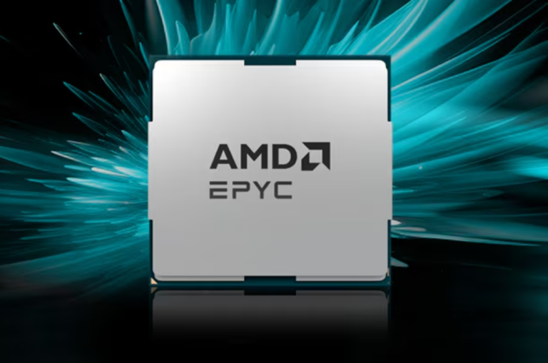
A cooler manufacturer’s product listing has revealed that AMD’s upcoming EPYC Verano AI host processor will use a soldered, non-removable socket architecture — a fundamental break from the field-serviceable design AMD has used for every prior EPYC server platform. The disclosure, made through Dynatron’s preliminary SB1-4U-ACTIVE heatsink listing and reported by Tom’s Hardware on Oct. 8, 2026, names AMD’s new platform as “Socket SB1” and associates it with EPYC 9006 LP processors targeting AI rack head nodes. The SB1 designation’s “B” is widely interpreted to indicate ball grid array packaging — meaning Verano will be soldered permanently to its server board, not seated in a removable socket. AMD has not yet independently confirmed the SB1 specification or the channel count.
What Dynatron’s Listing Actually Confirms
Dynatron, a Taiwan-based server cooling manufacturer, publishes preliminary cooler listings well before formal CPU launches to signal platform compatibility to its OEM customers. The company’s SB1-4U-ACTIVE listing — spotted by hardware tracker InstLatX64 and first covered on Oct. 8 — explicitly names support for “AMD EPYC Verano on Socket SB1,” giving the platform its first public name.
The listing associates Verano with up to 72 Zen 6 cores and a reported boost clock of 5 GHz. It also names LPDDR5X delivered through SOCAMM2 modules — the same field-replaceable memory standard AMD’s competitor Nvidia uses in its Vera Rubin platform. The cooler’s maximum supported processor TDP remains listed as “TBD,” indicating either AMD’s socket power definition or Dynatron’s thermal validation is not yet complete. All figures from this listing should be treated as preliminary until AMD publishes the official EPYC 9006 LP product stack, as Guru3D’s coverage noted.
The SB1-4U-ACTIVE unit itself is a 4U-format active cooler measuring 128.05 × 106.6 × 130.7 mm (5.04 × 4.20 × 5.15 in). It uses a vapor chamber and heat pipe design paired with an aluminum fin stack and a double-ball-bearing fan rated to 6,000 RPM and 91.7 CFM of airflow — specifications nearly identical to Dynatron’s J26 cooler designed for AMD’s much larger SP7 socket. Whether that is a design reuse or a placeholder pending finalized Verano thermal data remains unclear.
Soldered to the Board: What BGA Packaging Means for Data Centers
The most significant technical signal in the SB1 socket name is the letter “B,” which Spanish-language hardware outlet Profesional Review interpreted as indicating BGA packaging — a connection method in which an array of solder balls on the processor’s underside is permanently reflowed to matching pads on the motherboard.
This would be an operational departure from every prior EPYC server platform. AMD’s SP5, SP7, and SP8 sockets all use land grid array designs in which the processor is seated in a removable socket with flat contact pads, allowing the CPU to be replaced in the field if it fails or if a customer needs to upgrade to a higher-SKU chip. A BGA Verano would eliminate that option. If the CPU develops a fault or if a data center operator wants a higher-core-count configuration, the entire server board must be replaced — not just the processor.
The engineering rationale is straightforward. AI host CPUs like Verano are deployed in tightly controlled rack architectures with a small number of fixed SKU configurations rather than the broad menu of options typical of general-purpose EPYC families. In that environment, the BGA format’s advantages — smaller physical footprint, lower power-delivery impedance from shorter signal paths, and the ability to integrate high-bandwidth mobile-lineage memory closer to the processor die — outweigh the loss of field-swap capability that general-purpose server operators rely on. This mirrors the strategy Nvidia takes with its Grace and Vera CPUs, which are deployed as fixed-function components within the Vera Rubin rack system rather than as field-upgradeable processor sockets.
For data center operators evaluating Verano, the practical implication is that spare-parts inventory and failure-recovery procedures will need to be planned at the board level, not the CPU level — a model already familiar to hyperscale operators who manage GPU accelerator blades on a board-replacement basis.
How Verano’s Memory Architecture Stacks Up
The reported 24-channel LPDDR5X memory subsystem is the other distinctive claim from the Dynatron listing, and if confirmed by AMD it would represent the widest memory bus ever shipped on a server-class CPU.
For context, AMD’s current EPYC Venice SP7 — its new Zen 6 general-purpose server platform shipping in late 2026 — supports 16-channel MRDIMM memory bandwidth at 12,800 MT/s, delivering up to 1.6 TB/s per socket. Nvidia’s Vera CPU, the Arm-based AI host processor in the Vera Rubin platform, achieves 1.2 TB/s via SOCAMM2 modules on a 1,024-bit data path running LPDDR5X at 9,600 MT/s.
A Verano platform with 24 SOCAMM2 channels, each running at 128-bit data width, would yield a 3,072-bit total memory data path. At LPDDR5X speeds of 9,600 MT/s — the rate SK Hynix’s mass-produced SOCAMM2 modules support — that translates to a theoretical aggregate bandwidth of approximately 2.9 TB/s, nearly double Vera’s 1.2 TB/s and significantly ahead of Venice SP7’s 1.6 TB/s. AMD has not confirmed the speed, channel count, or exact bandwidth figure, and Guru3D flagged the uncertainties that the “actual capacity, channel arrangement, error-correction implementation and supported transfer rates have not yet been established.”
SOCAMM2 (Small Outline Compression Attached Memory Module 2) is a field-replaceable memory standard based on LPDDR5X that was purpose-built for AI servers. SK Hynix began 192GB SOCAMM2 mass production in April 2026 for Nvidia’s Vera Rubin platform, and AMD’s official May 2026 press release confirmed Verano would adopt the same standard, noting its “compact size and horizontal placement benefit modern AI server design” while acknowledging that reliability, availability, and serviceability (RAS) limitations would constrain early deployment scenarios.
One real-world cost signal worth noting: LPDDR5X contract prices rose approximately 90% quarter-over-quarter in the first quarter of 2026, a record quarterly increase for that memory type, as AI server platforms from both Nvidia and AMD accelerate adoption.
Socket SB1 in AMD’s Three-Socket Strategy
The SB1 discovery completes a picture of AMD running three distinct Zen 6 server socket families simultaneously in 2027 — a more fragmented platform strategy than any prior EPYC generation.
SP7 is the flagship general-purpose socket, supporting Venice processors with up to 256 Zen 6c cores, 16-channel DDR5/MRDIMM, and PCIe 6.0. Shipments are scheduled to begin in late 2026. SP8 targets mid-range general-purpose servers with Venice at up to 128 cores and 8-channel memory, expected in the first half of 2027. SB1 is the newcomer — a soldered, BGA socket for Verano, physically smaller than both and optimized specifically for the AI head-node role, with a 24-channel LPDDR5X subsystem that trades the configurability of LGA for density and bandwidth efficiency. AMD’s three-socket Zen 6 strategy creates a broader portfolio than any prior EPYC generation.
The three-socket model creates new qualification overhead for server OEMs and system integrators. Motherboards for SP7 and SP8 are incompatible with SB1; cooling solutions validated for SP7 must be re-validated for SB1 (as Dynatron is now doing with its SB1-4U-ACTIVE listing). Data centers planning 2027 infrastructure will need to account for separate spare-parts pools, separate management tooling profiles, and separate failure-mode procedures for each socket family — a consideration that will not appear in benchmark comparisons but will show up in total cost of ownership models.
Competing With Nvidia Vera: x86 vs. Arm
Verano enters a market where Nvidia’s Vera processor has already established a competitive baseline. Vera uses 88 custom Arm-based Olympus cores paired with 1.2 TB/s of LPDDR5X memory bandwidth and a Scalable Coherency Fabric delivering 3.4 TB/s of on-chip bisection bandwidth. Phoronix published independent Vera HPC benchmarks on Oct. 6, 2026, finding that Vera’s LPDDR5X 9,600 MT/s memory delivered especially strong results in memory-bandwidth-intensive workloads, outperforming AMD EPYC Turin and Intel Xeon in those specific scenarios — though Vera’s 88 core count placed it at a disadvantage in raw parallelism benchmarks against higher-core-count x86 parts.
AMD’s primary counter-argument is x86 compatibility. EPYC Venice launched in July 2026 with AMD claiming up to 3.3x higher general-purpose CPU server performance versus Vera across six workloads at a 100 kW rack power budget, as StorageReview documented at Advancing AI 2026. Enterprise workloads compiled for decades on x86 run natively on Venice and Verano without recompilation or re-qualification — a compatibility argument AMD has made explicitly and which has resonated with enterprise customers who manage large x86 software estates. Verano’s purpose-built design is intended to push the memory-bandwidth dimension of that argument further with its 24-channel LPDDR5X subsystem.
The fundamental architectural bet divides the AI host CPU market cleanly: Nvidia argues that Arm’s per-core power efficiency, combined with massive on-chip bandwidth and tight NVLink-C2C integration at 1.8 TB/s with Blackwell GPU accelerators, produces superior inference economics at the rack level. AMD argues that x86 compatibility reduces total deployment friction, and that Verano’s wider LPDDR5X bus narrows or erases the memory-bandwidth advantage Vera currently holds.
What Is SOCAMM2?
SOCAMM2 — Small Outline Compression Attached Memory Module 2 — is a field-replaceable server memory standard designed to bring LPDDR5X’s power efficiency and bandwidth density into AI server deployments without soldering memory permanently to the board. Where conventional LPDDR is bonded directly to the system-on-chip or the mainboard, SOCAMM2 packages the LPDDR5X dies in a removable module that operators can replace if a memory failure occurs — a significant serviceability improvement for AI server deployments.
SK Hynix, which began 192GB SOCAMM2 mass production in April 2026, states that SOCAMM2 delivers more than twice the bandwidth of conventional RDIMM and reduces energy draw by more than 75% for the memory subsystem. Those modules are currently shipping for Nvidia’s Vera Rubin platform; AMD’s confirmed adoption of the same standard for Verano means both major AI-CPU platforms will draw from the same memory supply chain by 2027.
The broader implication is a structural shift in how AI server memory is specified and sourced. RDIMM — the conventional server memory format based on DDR5 — remains the standard for general-purpose EPYC Venice servers. But for AI host CPUs where bandwidth per watt matters more than raw capacity, SOCAMM2’s combination of high bandwidth, low power draw, and field replaceability makes it the emerging industry default.
Launch Timeline
AMD plans to introduce Verano in the second half of 2027, paired with Instinct MI500-series GPU accelerators in AMD’s next-generation Helios rack-scale AI system, as ITPro reported from Advancing AI 2026. Venice SP7 processors are scheduled to begin shipping in the fourth quarter of 2026. Venice SP8 and Venice-X — the 3D V-Cache variant offering up to 1,152 MB of L3 cache at up to 96 cores — are expected through the first half of 2027.
What AMD has not yet disclosed publicly includes SB1’s physical dimensions, exact pin or pad counts, power delivery specifications, confirmed memory channel count, or the number of Verano SKUs planned. The socket’s existence is established through the Dynatron cooler listing — not through an AMD press release or product brief. Further technical detail is expected as Verano’s 2027 commercial launch approaches.
Frequently Asked Questions
What is the AMD EPYC Verano SB1 socket?
SB1 is the platform designation for AMD’s EPYC Verano AI host CPU, first publicly identified through a Dynatron server cooler listing in October 2026. The “B” in SB1 is widely interpreted to mean ball grid array packaging, which bonds the processor permanently to the server motherboard using solder balls rather than placing it in a removable socket. This is a departure from AMD’s standard EPYC server platforms (SP5, SP7, SP8), which all use removable land grid array sockets. AMD has not yet officially published the SB1 specification, confirmed the channel count, or released a full Verano product brief.
How does AMD Verano’s LPDDR5X memory compare to Nvidia Vera’s?
Both Verano and Nvidia’s Vera CPU use LPDDR5X memory delivered through SOCAMM2 modules. Nvidia Vera supports 8 SOCAMM2 modules on a 1,024-bit data path for 1.2 TB/s of aggregate bandwidth. AMD Verano is reported to use a 24-channel LPDDR5X configuration — 24 SOCAMM2 modules on a 3,072-bit data path — which, at LPDDR5X speeds of 9,600 MT/s, would yield approximately 2.9 TB/s of theoretical memory bandwidth. AMD has not officially confirmed the channel count, so this figure should be treated as preliminary until the full EPYC 9006 LP product stack is published.
What does BGA packaging mean for data center operators buying Verano servers?
It means the Verano CPU is soldered permanently to the server board and cannot be replaced individually. If a Verano processor fails or if an operator wants to move to a higher-core-count configuration, the server board must be replaced rather than just the CPU. This is already the standard operational model for GPU accelerator blades in AI racks, and it simplifies power-delivery design and manufacturing — but it requires data center spare-parts inventories and failure-recovery plans to be structured around board-level replacement rather than CPU-level swaps.
When will AMD EPYC Verano be available?
AMD plans to launch Verano in the second half of 2027, alongside the Instinct MI500-series GPU accelerators, as the CPU component of AMD’s next-generation Helios rack-scale AI system. Venice SP7, AMD’s general-purpose Zen 6 EPYC platform, is scheduled to begin shipping in the fourth quarter of 2026. Venice SP8 and Venice-X are expected through the first half of 2027.