HomeAuto TechInsights Teardown Confirms TSMC 2nm Nanosheet Transistors Now Inside iPhone 18 Pro
TechInsights Teardown Confirms TSMC 2nm Nanosheet Transistors Now Inside iPhone 18 Pro
September 24, 2026:
Techinsights.com
Analyst firm TechInsights published the first independent technical analysis of Apple’s A20 Pro processor on September 22, 2026 — and for the semiconductor industry, the significance goes well beyond a single iPhone chip. Until that report, every performance figure attached to TSMC’s 2-nanometer N2 process node — the 15 percent speed gain, the 30 percent power reduction, the 1.15× logic density increase over the prior 3nm generation — existed solely as the foundry’s own characterization data presented at academic conferences. TechInsights has now extracted the A20 Pro from an iPhone 18 Pro, independently measured production silicon, and published preliminary findings that transform those claims from foundry-asserted to independently validated. Every competitor building a 2nm-class chip now has an external benchmark to meet.
From Fin to Nanosheet: What Gate-All-Around Actually Changes
The headline finding is architectural. TechInsights confirmed that the A20 Pro deploys gate-all-around nanosheet transistors — a fundamental structural departure from the FinFET technology that has defined leading-edge semiconductor manufacturing since Intel introduced it in the early 2010s. ASML’s public documentation on GAA vs. FinFET design explains the underlying principle: whereas a FinFET gate wraps around a vertical silicon fin on three sides, leaving one face of the conducting channel exposed, gate-all-around nanosheets enclose the channel on all four sides simultaneously.
In a FinFET, that exposed face becomes an increasingly costly limitation as geometries shrink and off-state leakage current grows harder to control. TSMC’s N2 nanosheet architecture replaces those vertical fins with horizontal stacked silicon ribbons, allowing the gate to enclose the channel on all four sides simultaneously. The result is stronger electrostatic control and reduced leakage. The IEEE Spectrum TSMC IEDM 2024 report documents these architectural changes in detail.
The design also introduces manufacturing flexibility unavailable in the FinFET era. In a FinFET, drive current is adjusted only in coarse increments by multiplying the number of fins — one, two, or three. TSMC’s implementation, branded NanoFlex, allows nanosheet width to vary across logic cells on the same die, effectively enabling fractional-fin gradations, as the IEEE Spectrum N2 coverage describes. High-performance CPU cores can use wider nanosheets for maximum drive current; efficiency cores and general logic use narrower ones. The same wafer contains both, tuned at the cell level.
One structural detail in TechInsights’ early findings carries particular weight for process engineers: TSMC integrates inner spacers in nanosheet channels — a dielectric material placed between the nanosheet channels and the source/drain regions. Inner spacers suppress leakage and improve long-term scaling headroom by enhancing isolation between the gate and source/drain parasitic capacitance. TechInsights flags this as a structural differentiator between TSMC’s N2 implementation and competing GAA approaches.
Fabricating these structures requires substantially more complex process steps than FinFETs. Nanosheet formation begins with depositing alternating layers of silicon and silicon-germanium, then selectively etching away the silicon-germanium to leave suspended silicon ribbon channels that gate material subsequently surrounds. The difficulty of that selective removal — at dimensions measured in single-digit nanometers — is one reason TSMC’s Geoffrey Yeap, vice president of R&D and advanced technology, described N2 as four years of work at the 2024 IEEE International Electron Devices Meeting.
What Does 2nm Actually Mean?
A brief orientation is warranted. The “2-nanometer” label is a process-generation designation, not a measurement of any single physical feature on the chip. Modern node names stopped corresponding to literal transistor dimensions more than a decade ago; the number signals relative capability improvements in density, performance, and power efficiency compared to the prior generation. What those improvements actually look like in production silicon is determined by independent measurement — which is what makes TechInsights’ analysis consequential.
TSMC’s own data from the IEDM 2024 conference document N2 performance gains over N3E: up to 15 percent faster at identical power, or up to 30 percent more efficient at identical speed, combined with a logic density increase of more than 1.15×. An enhanced variant, N2P, is scheduled to enter mass production in the second half of 2026, with TSMC’s official N2P roadmap projecting roughly 18 percent additional speed or 36 percent additional efficiency improvement relative to N3E.
TechInsights’ exploratory analysis specifically notes that the A20 Pro uses aggressively scaled nanosheet logic cells. The complete subscriber report will provide transistor-level measurements — critical dimensions, gate pitch, SRAM cell density — that will constitute the definitive external record of what TSMC N2 produces in production silicon.
Inside the Die: Same Footprint, More Compute
TechInsights’ preliminary floorplan analysis places the A20 Pro compute die at approximately 8.0 mm by 12.3 mm (0.31 by 0.48 inches), yielding an estimated A20 Pro die area of 98.2 mm² (0.152 square inches) — nearly identical to the A19 Pro it replaces. That Apple maintained essentially the same die footprint despite a generational process shrink is itself a choice: N2’s density gains are being spent on additional compute rather than a smaller die.
TechInsights confirmed a six-core CPU — two high-performance cores with dedicated L2 cache each, and four efficiency cores sharing cache across multiple banks. The A20 Pro GPU core count expands to seven cores, one more than the previous generation.
The most structurally significant expansion is in neural processing. Apple claims doubled AI chip performance over the A19 Pro, and TechInsights’ preliminary floorplan analysis confirms that the neural processing area has grown substantially relative to the prior generation. The chip carries dual 16-core Neural Engines alongside Neural Accelerators integrated directly within the CPU complex — a distributed architecture that routes AI workloads to compute throughout the die rather than funneling them through a single centralized block. Apple also claims 50 percent more memory bandwidth in the A20 Pro relative to the A19 Pro — a figure that points toward the packaging shift documented in the next section.
Why Apple Moved the Memory Sideways
For years, Apple stacked LPDDR memory directly atop the application processor die in a package-on-package arrangement, placing memory above the chip in a compact vertical footprint. The A20 Pro abandons that vertical stack.
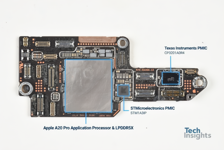
TechInsights’ preliminary analysis identifies a WMCM side-by-side package in which the processor and DRAM are positioned side by side within the same wafer-level package rather than vertically stacked. Preliminary analysis points to a 96-bit LPDDR5X memory interface — a wider memory bus than a vertical stack arrangement could practically accommodate without significant signal-routing complexity.
The motivation for this shift is threefold. Positioning memory beside the processor rather than above it removes the memory’s thermal load from the chip’s hottest region — a persistent constraint in mobile package-on-package designs. A side-by-side layout physically enables a wider memory interface without stacking-imposed signal-routing penalties. And at the wafer level, integrating two die side by side allows each component to be tested independently before assembly, which can improve overall package yield.
Apple’s redesigned vapor chamber cooling system — which the company says provides 3x more surface area than the iPhone 17 Pro’s and up to 40 percent better sustained performance — is partly enabled by this packaging shift, which eliminates the memory as an obstacle between the chip and its cooling surface.
Supply chain reports from late 2025 confirmed Apple secured TSMC 2nm majority capacity for 2026, covering the A20 and A20 Pro for the iPhone 18 line as well as M6 chips for the next MacBook Pro generation and R2 chips for a refreshed Vision Pro. TSMC’s production facilities in Baoshan and Kaohsiung, Taiwan, were producing approximately 50,000 N2 wafers per month at the production launch, with capacity projected to reach 100,000 wafers per month by the end of 2026. Those wafers carry a $30,000 N2 wafer price — roughly double the price of TSMC’s 3nm wafers — reflecting both the process complexity and the captive demand from Apple and other early customers.
Is TSMC N2 the Strongest 2nm Process Now in Production?
TSMC is not the only foundry to have introduced a 2nm-class gate-all-around process. The comparison with Samsung and Intel illuminates both where TSMC leads at scale and where rivals are making different architectural bets.
Samsung was technically first to deploy gate-all-around transistors commercially, beginning with its SF3 3nm process in 2022. Its SF2 2nm process entered mass production in late 2025, producing the Exynos 2600 chip for the Samsung Galaxy S26. Independent reports indicate Samsung SF2 yields crossed 50 percent in January 2026. TSMC’s N2 yields, by contrast, were placed well above 60 to 70 percent by Ming-Chi Kuo’s yield analysis of TF International Securities as early as spring 2025 and continued to improve through the production ramp. On the process architecture side, TechInsights’ early findings flag TSMC’s inner spacers versus Samsung — a distinction with implications for leakage control and scalability that the full October report will quantify.
Intel’s 18A process represents the most architecturally aggressive bet in the 2nm class. Its RibbonFET with PowerVia backside power moves power connections from the front surface of the chip to the rear of the silicon substrate. Separating power from signal wiring substantially reduces voltage droop and enables tighter circuit packing — an advantage Intel is specifically targeting at AI data-center workloads. Neither TSMC N2 nor Samsung SF2 includes backside power delivery; TSMC’s equivalent technology, Super PowerRail, is expected with the A16 node projected for the second half of 2026. The tradeoff is complexity: designing for backside power delivery requires a significant departure from the front-side assumptions embedded in years of existing EDA tools and SoC IP. The designers adapting existing mobile or PC architectures to N2 face fewer migration barriers than those moving to Intel 18A.
In the dimension that matters most right now — confirmed commercial availability, volume, and independent external measurement — the A20 Pro in the iPhone 18 Pro and Pro Max sets the reference point. TSMC N2 is in people’s pockets, and it now has a teardown to show for it.
What the October 14 Webinar Will Add
TechInsights is scheduled to present a deeper examination of the A20 Pro at a free public iPhone 18 Pro webinar on October 14, 2026 at 11:00 a.m. ET, covering die architecture, packaging details, the Apple C2 modem and N1 Wi-Fi chip, component costs, and process comparisons with Intel and Samsung drawn from TechInsights’ reverse engineering. Registration is open to the public at no cost; the session will also be made available on demand.
TechInsights has already published a iPhone 18 Pro Max preliminary teardown from September 18, 2026, which identified the Qualcomm X80 modem and Apple’s own N1 Wi-Fi chip among the major components alongside the A20 Pro. The complete A20 Pro analysis — including transistor-level measurements, SRAM cell scaling, and direct process comparisons — is available on the TechInsights Platform to registered subscribers. What TechInsights has published so far is enough to establish a new reference point for the industry: TSMC N2, with gate-all-around nanosheet transistors, inner spacers, and a side-by-side memory architecture, has been independently confirmed at consumer mass-market scale. Every competitor building a 2nm-class chip now knows what the benchmark looks like from the outside.
Frequently Asked Questions
What makes gate-all-around nanosheet transistors different from the FinFETs in earlier iPhone chips?
FinFET transistors — which Apple used through the A19 Pro in the iPhone 17 series — have a vertical silicon fin at their core, with the gate wrapping around three sides of the conducting channel. Gate-all-around nanosheet transistors replace that vertical fin with horizontal stacked silicon ribbons and surround the channel on all four sides. The additional contact between gate and channel gives engineers tighter electrostatic control, reducing the leakage current that wastes power when the transistor is supposed to be switched off. At the miniaturization required for a 2nm-class process, that four-sided gate control is essential; the FinFET’s three-sided approach no longer provides sufficient control over current at these dimensions.
How does TSMC’s N2 compare to Samsung SF2 and Intel 18A, and which is better?
All three use gate-all-around architectures, but they differ in manufacturing execution and design philosophy. TSMC N2 uses inner spacers for leakage control, retains front-side power delivery, and achieved production yields that independent analysts placed well above 60 to 70 percent before the iPhone 18 launch — allowing Apple to commit the majority of initial capacity for the world’s highest-volume premium smartphone. Samsung’s SF2 entered mass production in late 2025 with yields reported around 50 percent as of early 2026, and it too retains front-side power delivery. Intel’s 18A is the architectural outlier: its RibbonFET gate-all-around transistors pair with PowerVia backside power delivery, physically separating power and signal wiring in a way neither TSMC N2 nor Samsung SF2 does yet. That separation enables lower voltage droop and tighter logic packing at the cost of a steeper design-migration burden. TSMC’s equivalent backside power technology is expected with the A16 node in the second half of 2026. The practical advantage currently belongs to TSMC in terms of confirmed volume and independent verification.
Why does it matter that TechInsights — not TSMC or Apple — published these findings?
TSMC’s published N2 performance numbers come from characterization data the company presented at the IEEE International Electron Devices Meeting using TSMC-selected test structures in a controlled academic setting. Apple does not disclose which foundry makes the A20 Pro, what process technology it uses, or what the die dimensions are. Until TechInsights extracted the chip from an iPhone 18 Pro and measured it, the industry was working from the foundry’s own unaudited claims. Independent reverse engineering translates those claims into verified data: actual die area, functional block allocation, packaging construction, and transistor architecture measured by a third party with no commercial interest in validating TSMC’s characterization. That distinction matters for every chip designer, investor, or competitor evaluating whether to commit a future product to a specific process node.
What questions will the full TechInsights report and October 14 webinar answer that the preliminary findings do not?
TechInsights’ preliminary findings establish the die dimensions, confirm the CPU and GPU core counts, identify the WMCM packaging architecture, and flag the gate-all-around inner-spacer structure. The full subscriber report and the October 14 webinar are expected to address precise transistor critical dimensions and gate pitch, SRAM cell density and scaling data relative to N3, the architecture of Apple’s C2 modem and N1 Wi-Fi chip, detailed component supplier identification, a component cost breakdown, and direct transistor-level comparisons with Samsung SF2 and Intel 18A. Whether the 96-bit LPDDR5X memory interface identified in preliminary analysis is definitively confirmed will also be addressed.