HomeAuto Samsung LPDDR6 Passes Snapdragon 8 Elite Extreme Gen 6 Validation for 2027 Flagships
Samsung LPDDR6 Passes Snapdragon 8 Elite Extreme Gen 6 Validation for 2027 Flagships
September 24, 2026:
Samsung.com
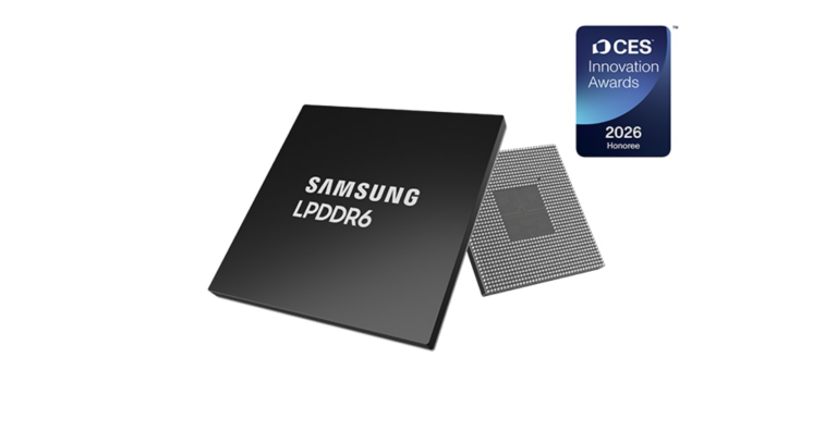
Samsung Electronics has completed the semiconductor industry’s industry-first LPDDR6 validation of LPDDR6 mobile DRAM on Qualcomm Technologies’ Snapdragon 8 Elite Extreme Gen 6 platform, clearing the commercial path for the next generation of mobile memory to appear in premium Android smartphones in 2027. The certification — announced during Qualcomm’s Snapdragon Summit 2026, which is currently underway in Maui, Hawaii — confirms that Samsung’s LPDDR6 can meet the full platform-level demands of Qualcomm’s most powerful mobile chip: not just component benchmarks, but signal integrity, timing closure, and thermal stability operating together in a real SoC environment.
That distinction matters. A memory chip passing component tests is different from a memory chip passing platform validation. OEMs and device makers do not commit to a memory generation until a chipmaker has certified that the combination works at the SoC level — which is precisely what this week’s announcement provides. For any phone buyer planning an Android upgrade in 2027, that certification is now done.
What LPDDR6 Actually Does Differently — and What It Doesn’t
The starting-speed number requires context that the announcement does not supply. Samsung’s validated LPDDR6 operates at up to 10.7 Gbps per pin — the same peak speed already reached by the most advanced current-generation LPDDR5X modules. The per-pin plateau is intentional: the LPDDR6 standard, formalized by JEDEC in its JESD209-6 specification published in July 2025, begins at 10.7 Gbps and scales toward a ceiling of approximately 14.4 Gbps in future iterations. Samsung’s 12-nanometer (nm) LPDDR6 is the baseline implementation of that standard.
What differentiates LPDDR6 from LPDDR5X at the same per-pin speed is its expanded input/output (I/O) architecture. LPDDR6 uses more I/O channels per die than LPDDR5X, which means total memory bandwidth scales beyond what per-pin speed alone would suggest. The result: Samsung’s validated 16-gigabyte (GB) LPDDR6 delivers 114 GB/s bandwidth on the Snapdragon 8 Elite Extreme Gen 6. For reference, LPDDR5X in current-generation Android flagships typically delivers approximately 77 to 83 GB/s. The 37% bandwidth increase comes not from faster individual pins but from more pins working in parallel.
This architectural distinction matters for AI. During large language model (LLM) inference on a phone — the process by which a device generates responses to queries or executes multi-step agent tasks — the processor repeatedly fetches large weight matrices and key-value (KV) cache data from memory. Research in the AI systems community has established that mobile LLM inference is bandwidth-bound: the chip spends more time waiting for data from memory than it does processing that data. Higher bandwidth compresses that wait. At 114 GB/s, LPDDR6 allows the Extreme Gen 6’s Hexagon NPU to access the data it needs for AI processing significantly faster than any phone has previously managed.
How LPDDR6 Manages Power During AI Workloads
Higher bandwidth would be an engineering tradeoff if it came at a proportional power cost. It does not — and the mechanism that explains why is one of LPDDR6’s more consequential advances.
Samsung’s LPDDR6 incorporates two cooperative power-management systems: Dynamic Voltage and Frequency Scaling (DVFS) and a new feature called Dynamic Efficiency Mode (DEM). DVFS is a technique that reduces both the operating voltage and the clock frequency of the memory subsystem in response to lighter workloads — a mechanism used in mobile DRAM since LPDDR5. DEM extends this further by selectively reducing power draw during lower-utilization periods between intensive inference steps, targeting the idle intervals within a longer AI session rather than only the average across the full task. Samsung’s documentation of DVFS and Dynamic Efficiency Mode covers both mechanisms.
The combined effect, according to Samsung’s internal laboratory testing under standard benchmarks, is a 21% efficiency gain over LPDDR5X. That figure carries the standard caveat that Samsung itself applies: internal test results do not guarantee identical real-world performance, which varies with device configuration and thermal management. Independent third-party testing will be needed once retail devices ship. But the directional improvement is significant: a memory subsystem delivering substantially more bandwidth while drawing meaningfully less power addresses one of the persistent tensions in on-device AI design, where both performance and battery life must improve simultaneously.
PRAC: Reliability for AI Agents Running Long Sessions
A third architectural advance in LPDDR6 addresses a more technical reliability concern that becomes commercially important specifically because of how AI agents operate.
Per-Row Activation Counting, or PRAC, is a mechanism that monitors how frequently specific memory rows are accessed during a session. Dense, repeated access to particular rows in DRAM can create electromagnetic interference that risks flipping data bits in adjacent rows — a vulnerability class known as Rowhammer, which affects all DRAM generations to varying degrees. PRAC counts activations and, when a row approaches a threshold suggesting elevated interference risk, triggers a targeted refresh of adjacent rows before any data integrity problem occurs.
PRAC has appeared in prior LPDDR specifications, but its relevance has grown with AI agents. Unlike a quick voice query or a photo generation task, an AI agent maintaining context across a long user session — tracking earlier steps in a multi-stage task, holding a growing KV cache — keeps the memory subsystem engaged intensively for minutes or hours rather than seconds. These sustained workload patterns produce exactly the kind of concentrated row-activation patterns that PRAC is designed to detect. For devices whose commercial pitch centers on persistent on-device AI agents, PRAC is less an abstract security feature than a practical reliability guarantee.
The Platform Validation Process — and What It Actually Certifies
The announcement’s phrase “industry-first validation” describes something more specific than a performance benchmark. Platform validation is the joint engineering process through which a memory maker and a chipmaker confirm that a memory product meets all the requirements of a specific SoC, not just its own standalone specifications.
That process covers signal integrity (whether the electrical signals between DRAM and SoC maintain quality at speed), timing closure (whether the memory’s latency characteristics fit the SoC’s memory controller design), power delivery (whether voltage rails are stable under the combined load of the SoC and memory operating together), and thermal behavior (whether the pair can sustain performance under the temperatures a phone generates). Passing all of those tests jointly is what enables OEMs to commit to a memory generation in production hardware — and what the Samsung LPDDR6 platform certification delivers for the Extreme Gen 6.
“We are proud to have successfully completed sampling and validation of LPDDR6 on Qualcomm Technologies’ next-generation mobile platform, following Samsung’s industry-first LPDDR6 development,” said Jangseok Choi, Vice President, Product Planning Team, Memory Business at Samsung Electronics. “This achievement demonstrates both the technology leadership and product readiness of our LPDDR6.”
Salman Saeed, Vice President of Product Management at Qualcomm Technologies, described the milestone from the platform side: “The successful validation of Samsung’s LPDDR6 memory on Snapdragon 8 Elite Extreme Gen 6 demonstrates the close collaboration between Qualcomm Technologies and Samsung to advance next-generation mobile technologies. LPDDR6 delivers the bandwidth and power efficiency needed to support increasingly sophisticated on-device AI experiences.”
Where This Leaves the Competition
Samsung is first to complete LPDDR6 platform validation on a next-generation mobile SoC, but it is not the only company developing the standard. SK hynix has announced LPDDR6 development based on its sixth-generation 10-nanometer-class process, which the company refers to as “1c.” SK hynix’s roadmap targets a peak transfer rate of 14.4 Gbps — 35% faster than the 10.7 Gbps baseline — with mass production in H2 2026. Micron is also working in the LPDDR6 space, though its specific mobile roadmap and timeline for platform validation have not been publicly confirmed.
Samsung’s competitive advantage at this moment is twofold: it completed the first platform certification with Qualcomm’s flagship chip, and its 12nm LPDDR6 is already available in the sampling and validation phase. SK hynix’s higher-ceiling product may reach consumers later. Whether Samsung retains the premium memory slot in 2027 flagship devices or whether SK hynix closes the gap before Galaxy S27 production commitments are made will determine the memory-market outcome of this generation.
Does the Snapdragon 8 Elite Gen 6 Also Get LPDDR6?
Not on the standard model. The Snapdragon 8 Elite Extreme Gen 6 and the standard Snapdragon 8 Elite Gen 6 are distinct silicon designs launched simultaneously at this week’s Summit, and the two differ in their memory support. The Extreme Gen 6 supports LPDDR6 (and backward-compatible LPDDR5X), while the standard Gen 6 supports LPDDR5X only.
This creates a memory-tier split within 2027’s Android flagship class. Devices built on the standard Gen 6 — expected to include mid-tier Ultra phones and many regional variants — will carry LPDDR5X, which remains a capable standard. The 114 GB/s bandwidth advantage, and the PRAC reliability guarantee for long-session AI agents, will be exclusive to Extreme Gen 6 devices until LPDDR6 migrates down the platform stack.
What Devices Will Carry LPDDR6 — and When
Samsung has not officially confirmed any device program using the validated LPDDR6 configuration. The commercial trajectory, however, is not ambiguous. Reports from multiple industry sources have indicated that Samsung has been testing LPDDR6 for the Galaxy S27 Pro and Galaxy S27 Ultra, the models that would historically pair with the highest-tier Qualcomm platform available. Lower-specification Galaxy S27 variants are expected to use different memory or processor configurations.
The Xiaomi 18 series has also been widely reported as an early Extreme Gen 6 device, with Xiaomi scheduled to hold a launch event this week. If those projections hold, LPDDR6 could reach consumer hands in the first quarter of 2027 — less than 18 months after JEDEC ratified the standard. That is a notably compressed generational cycle: it took LPDDR5 roughly five years from standard ratification to mass-market consumer availability. Samsung’s accelerated development and early platform validation have compressed that timeline substantially.
Additional technical and commercial details from Samsung and Qualcomm are expected to be disclosed before Snapdragon Summit 2026 concludes on September 24.
What Does This Mean for a Reader Buying a Phone in 2026 vs. 2027?
For a reader considering a flagship Android purchase now, the practical decision point is clear: current 2026 flagships carrying LPDDR5X will not receive LPDDR6 through a software update. The memory architecture is fixed in hardware. A purchase made this year is a purchase of the LPDDR5X generation. Waiting for Q1 2027 Extreme Gen 6 devices means gaining both the validated LPDDR6 memory stack and the Extreme Gen 6’s AI inference architecture — a combination that represents the most significant memory-layer upgrade the Android ecosystem has seen in several years.
For readers who already own a current flagship and are satisfied with its AI performance, the 114 GB/s figure has limited urgency: the AI features on 2026 devices are already delivering more capability than most users currently exercise. But for users who plan to rely on AI agents, extended-context applications, or any workload that runs inference continuously over long sessions, PRAC-backed LPDDR6 represents a genuine qualitative improvement over what currently ships.
Frequently Asked Questions
What is the difference between LPDDR6 and LPDDR5X?
LPDDR6 and LPDDR5X share a similar starting per-pin speed — both reach 10.7 Gbps in their current implementations — but LPDDR6 uses an expanded I/O architecture that delivers significantly more total bandwidth: 114 GB/s in Samsung’s validated configuration, compared to roughly 77–83 GB/s from current LPDDR5X designs. Beyond bandwidth, LPDDR6 introduces Dynamic Efficiency Mode (DEM) for finer-grained power management during AI workloads, and Per-Row Activation Counting (PRAC) for sustained reliability during the extended memory-access sessions that AI agents generate. LPDDR6 is also designed to scale to 14.4 Gbps per pin in future iterations, widening the performance gap over time.
When will phones with LPDDR6 memory be available?
Consumer devices carrying LPDDR6 are projected to arrive in the first quarter of 2027, beginning with flagships built on the Qualcomm Snapdragon 8 Elite Extreme Gen 6 platform — the specific chip on which Samsung completed its validation this week. The Samsung Galaxy S27 Pro and Galaxy S27 Ultra are widely reported as candidates for LPDDR6, though Samsung has not officially confirmed the configuration. Xiaomi’s 18 series, which is expected to be announced in the near term, is also a likely early LPDDR6 device.
Does the standard Snapdragon 8 Elite Gen 6 also support LPDDR6?
No. Qualcomm launched two distinct silicon designs at Snapdragon Summit 2026: the Snapdragon 8 Elite Extreme Gen 6 and the Snapdragon 8 Elite Gen 6. LPDDR6 support is exclusive to the Extreme Gen 6 — the higher-end design that also includes an Adreno 850 GPU, 18 MB of on-chip GPU memory, and a stronger Hexagon NPU. The standard Gen 6 supports LPDDR5X only. Phones built on the standard chip will not carry LPDDR6, regardless of the phone’s price tier.
Why does LPDDR6 matter specifically for on-device AI agents — not just faster apps generally?
Conventional smartphone apps load code and data into memory once and largely keep it there. AI inference workloads — especially AI agents that maintain context across a long session — continuously fetch large model weights and growing KV cache data from DRAM. Memory systems research has established that this class of workload is memory-bandwidth-bound: the processor completes calculations faster than it can load the next dataset from memory. LPDDR6’s 37% bandwidth increase over current LPDDR5X directly addresses this bottleneck. The PRAC reliability mechanism matters equally: an agent holding a large context for hours applies concentrated activation patterns to specific memory rows, and PRAC prevents the data integrity risks that such patterns can create.