HomeAuto TuringQ Gen3 Claims Quantum Advantage: Single TFLN Chip Logs 11,059 Photons in One Millisecond
TuringQ Gen3 Claims Quantum Advantage: Single TFLN Chip Logs 11,059 Photons in One Millisecond
September 13, 2026:
Turingq.com
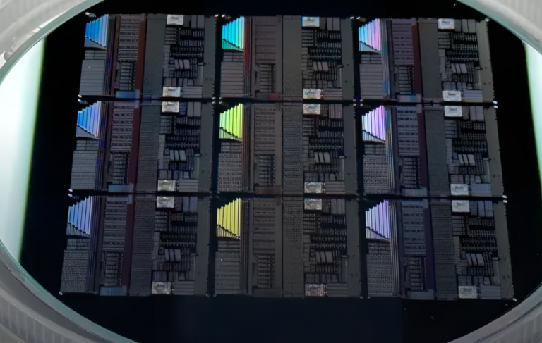
A Shanghai photonics startup is today unveiling the most photon-dense on-chip Gaussian boson sampling system ever demonstrated, built on a single thin-film lithium niobate chip and operating inside a standard data center rack — no cryogenic cooling required for the processor itself. The system, called Zhiyuan 3.0 by its research team and marketed as the TuringQ Gen3, recorded up to 11,059 photon detection events in a single one-millisecond sampling run at the 19th Pujiang Innovation Forum (September 11–14, 2026), and classically simulating that output at full scale would require an estimated 9.7 million years on a GPU farm. For technically literate readers evaluating this claim: the underlying physics paper was posted to arXiv on September 10 and has not yet undergone peer review. Neither has it been independently replicated. The headline figure is real in the sense that the team’s preprint describes a coherent experimental methodology and validated output statistics — but the field’s standard for treating a benchmark as established requires peer review, and that process is pending.
What the arXiv paper establishes — and what the draft marketing materials for the Gen3 do not fully explain — is why this chip achieves what previous photonic systems could not, and where the remaining engineering gaps are.
What TFLN Enables That Silicon Photonics Cannot
The enabling material is thin-film lithium niobate, referred to in the field as TFLN. This is not a new material, but a new form of an old one. Lithium niobate in bulk crystal form has underpinned optical communications for decades, appearing in the modulators at the core of fiber-optic networks. In thin-film form, where a 400-nanometer (0.000016-inch) monocrystalline layer of lithium niobate is bonded onto a buried oxide substrate, the physics change in a commercially useful way, as documented in a 2025 TFLN quantum photonics review published by researchers at the Technical University of Denmark.
The primary advantage is electro-optic modulation speed. TFLN’s Pockels effect — its native nonlinear response to an electric field — is large enough that in thin-film waveguides, the modulation bandwidth achievable at low drive voltage far exceeds what silicon photonics or silicon nitride platforms currently deliver. The Zhiyuan 3.0 chip reports a 67 GHz electro-optic bandwidth at a half-wave voltage of 3.18 volts, enabling a clock rate of 4 GHz — the highest reported in any quantum system. Silicon photonic modulators typically achieve roughly 25 to 30 GHz bandwidth, and at higher drive voltages.
For a quantum computing system, that modulation speed is not a cosmetic advantage. It determines how densely time-bin windows can be packed. In the Zhiyuan 3.0 architecture, each time-bin window is 250 picoseconds (about a quarter of a nanosecond). At 4 GHz, thousands of distinct time bins fit inside a single millisecond sampling run. Each time bin is treated as a separate computational mode. The chip therefore generates a computing network whose effective size vastly exceeds the number of physical optical components — and that is the entire point of the space-time multiplexing approach.
Additionally, TFLN’s waveguide transmission loss is exceptionally low. The Zhiyuan 3.0 chip reports propagation loss and coupling efficiency of 0.03 dB per centimeter and fiber-to-chip coupling loss of 0.9 dB per facet at 1,550 nanometers (0.00006 inches), both verified by the arXiv paper’s device characterization section. Loss is the central adversary of photonic quantum advantage: every photon lost is a computation error, and classical simulation of GBS becomes easier as system loss increases. The 2024 Nature Physics paper by Oh et al. established a stricter classical simulation threshold specifically because earlier GBS experiments operated at high loss. TuringQ’s paper claims to satisfy the new stricter criterion, with an effective squeezed photon number N_eff of approximately 117.9, placing classical simulation requires 9.7 million GPU-years on NVIDIA A100 hardware.
What Space-Time Multiplexing Does — and How It Differs From OptQC’s Approach
Photonic quantum computing has two scaling strategies for generating large computational mode networks without exponentially multiplying hardware. Pure time-domain multiplexing (TDM), used by Japan’s OptQC and developed at the University of Tokyo’s Furusawa laboratory, encodes sequential qubits as light pulses at different times through the same set of optical components. Space-time multiplexing (STM), deployed in the Zhiyuan 3.0 chip, adds a second axis: the photon evolves across both spatial optical modes (parallel waveguide paths) and temporal modes (time-bin windows) simultaneously.
The practical consequence is that the mode count scales as the product of spatial modes multiplied by time steps, not as either dimension alone. The Zhiyuan 3.0 chip uses four spatial modes and runs for many time steps per sampling run, generating a space-time entangled cluster state with space-time entanglement. In the quantum advantage benchmark simulation, the team models 10,000 time steps with four spatial modes, totaling 40,000 modes, and demonstrates that classical simulation at this scale requires a bond dimension of approximately 10,000 and computation exceeding 9.7 million GPU-years on NVIDIA A100 hardware.
The architectural difference from OptQC’s approach is not merely technical — it reflects a different theory of how quantum computing scales. OptQC’s TDM uses continuous-variable squeezed light and targets fault-tolerant universal quantum computing via Gottesman-Kitaev-Preskill (GKP) error correction, with a GKP error correction roadmap to one million logical qubits by 2030 backed by NTT’s IOWN fiber-optic infrastructure investment. TuringQ’s STM approach uses the same squeezed vacuum input but targets programmable near-term quantum acceleration for specific task classes — Gaussian boson sampling for graph optimization, drug discovery, and AI reservoir computing — rather than fault-tolerant universal computation.
Neither approach is further ahead on the ultimate goal of fault tolerance, because both face the same underlying challenge: photon loss and error correction in optical systems remain unsolved at scale.
What the Chip Actually Demonstrated vs. What the Marketing Claims
TuringQ’s commercial materials describe the Gen3 as supporting “10,000-photon-scale resources across one million computational modes.” The arXiv paper provides more precise numbers. The demonstrated maximum is maximum 11,059 photon detection events in a single one-millisecond sampling run at 300 mW pump power. The one million modes figure is the architecture’s theoretical scale ceiling based on the TFLN chip’s design parameters — it is an engineering projection, not a measurement.
A more significant distinction involves the detector system. The draft marketing materials describe the Gen3 as a “single-chip” system integrating four hardware modules including single-photon detection. What the arXiv paper describes is a chip that integrates quantum source (squeezed vacuum injection), programmable photonic processing (the multi-layer MZI network with delay loops), and quantum-classical control — but 16 SNSPD channels off-chip require cryogenic cooling. The processor operates at room temperature; the detectors do not. Fully integrating high-efficiency single-photon detectors on-chip is identified in the paper itself as a key remaining engineering challenge — along with on-chip integration of the squeezed light source — before true single-chip operation is achievable.
The paper’s fabrication process is documented in detail: 6-inch x-cut TFLN wafers from NanoLN, 400 nm lithium niobate layer on 4.7 micrometer (0.00019-inch) buried oxide, waveguides patterned by deep-ultraviolet (KrF) scanner and etched 200 nm via argon-plasma etching, 1,200 nm silicon oxide cladding, titanium nitride heaters, gold electrodes. The team spent 4.5 years establishing the wafer-scale TFLN fabrication process at the CHIPX pilot line in Wuxi, Jiangsu, which can process 12,000 six-inch wafers annually, according to TuringQ CHIPX pilot line production coverage. That production investment is, arguably, the more durable industrial achievement behind today’s announcement.
Validation: What the Team Confirmed and What Independent Review Still Needs to Assess
The Zhiyuan 3.0 paper validates its output statistics through three independent methods. First, it compares second-order photon correlation validation against four theoretical models — GBS, thermal light, coherent light, and squashed state — and shows only the GBS model matches the experimental data. Second, it measures few-photon probability distribution fidelities for single-photon, two-photon bunching, and two-photon non-bunching events, reporting 0.9978, 0.9962, and 0.9911 respectively. Third, it runs a Bayesian counter analysis in which the GBS hypothesis becomes progressively more distinguishable from every spoofer model as sample count increases.
These are the standard validation methods for GBS experiments, and the methodology is coherent with the broader literature. The team also used DeepQuantum, TuringQ’s own quantum simulation framework, to verify theoretical predictions — which, as with any experiment where proprietary software is used for validation, will warrant independent reproduction in peer review.
On the quantum advantage claim specifically: the team applies the Oh et al. (2024) classical simulation threshold to their system parameters and concludes that classical simulation at N_eff ≈ 117.9 requires a matrix product state bond dimension of approximately 10,000 and computation time of 9.7 million GPU-years. Whether independent reviewers accept those parameters as accurately reflecting the experimental conditions is the open question.
Beyond Sampling: GBS as an AI Accelerator
The part of the Zhiyuan 3.0 paper that has received less attention in initial coverage is its demonstration of the chip as a practical computation engine for a task beyond GBS benchmarking. The team reconfigured the same chip — without hardware changes — as a “GBS-powered world model” for predicting Kármán vortex street fluid dynamics, a standard benchmark problem in computational physics, achieving GBS-powered fluid dynamics prediction results that outperform classical alternatives.
The photonic quantum model achieved lower mean squared error than a classical echo state network (ESN) baseline at every tested ESN size from 5 to 320 nodes, while using 84.1% fewer trainable readout parameters than the 320-node ESN. The photonic model mapped 50 measured features to five predicted outputs using 255 trainable parameters; the 320-node ESN required 1,605. This is a modest but concrete demonstration that the same hardware used for GBS advantage benchmarking can also act as a parameter-efficient dynamical system predictor — a step toward the “quantum reservoir computing” applications that multiple photonic quantum companies have proposed as the near-term use case for GBS hardware.
The significance is architectural: GBS chips whose sole function is demonstrating sampling advantage have no commercial value. A GBS chip that can be reconfigured for AI inference tasks, fluid dynamics modeling, or financial graph optimization — using the same TFLN hardware through software reconfiguration — is a different product proposition. Whether the advantage generalizes beyond this specific benchmark remains undemonstrated.
Where TuringQ Sits in the Global Photonic Quantum Landscape
The photonic quantum computing field is now segmented by three distinct architectural choices: material platform (TFLN vs. silicon photonics vs. silicon nitride vs. fiber-optic), computation model (discrete-variable photon-counting for MBQC or FBQC vs. continuous-variable squeezed light for GBS or CV quantum computing), and scaling strategy (space-time multiplexing vs. TDM vs. growing physical chip footprint).
TuringQ’s TFLN + STM + GBS positioning is architecturally distinct from its nearest comparison points:
PsiQuantum (United States, backed by A$940 million in Australian government funds and a $100 million CHIPS Act commitment) uses silicon photonics at GlobalFoundries to pursue fusion-based quantum computing with discrete-variable single photons. Its February 2025 Nature paper demonstrated 99.22% silicon photonic fusion fidelity on a system architecture oriented toward fault-tolerant universal computation rather than near-term GBS advantage.
ORCA Computing (United Kingdom) uses time-domain multiplexing in fiber-optic loops at room temperature, targeting practical GBS applications but on a different physical substrate — its PT-3 system is expected in 2026 without on-chip integration.
OptQC (Japan, NTT-backed) uses TDM with continuous-variable squeezed light on a room-temperature free-space optical platform, targeting one million logical qubits via GKP error correction by 2030 — a universal quantum computing roadmap rather than a near-term GBS accelerator.
The Guizhen Chip and USTC silicon photonic chip demonstrated in August 2026 uses discrete-variable measurement-based quantum computing on silicon with high-dimensional path encoding — a categorically different approach that achieved Guizhen Chip 98.7% Grover accuracy from four photons but is not a GBS system.
Among chip-scale GBS demonstrations specifically, the Zhiyuan 3.0 / TuringQ Gen3 claim of 11,059 photons in 1 millisecond on a single TFLN chip would, if peer-reviewed and confirmed, represent the largest on-chip photon count in any GBS experiment. Prior chip-scale GBS demonstrations peaked at far lower photon counts. The Jiuzhang 4.0 system that reached 3,050 photons in free-space bulk optics used a different, multi-component architecture that cannot be hosted in a data center rack, as documented in the Jiuzhang 4.0 photonic GBS result by USTC’s Pan Jianwei group.
Business Context: Funding, Valuation, and IPO Ambitions
TuringQ has raised nearly 1 billion yuan (approximately $149 million USD) in 2026 alone across two funding rounds, following a Series C that closed in April and pushed the company’s valuation above 7 billion yuan (approximately $1.04 billion USD), as reported in TuringQ IPO tutoring CSRC filing coverage. The National Venture Capital Guidance Fund’s Yangtze River Delta Fund made its first direct investment in the quantum technology sector through TuringQ, a choice that signals the level of state-directed confidence in the company’s trajectory.
In August 2026, TuringQ filed for IPO tutoring with the Shanghai branch of the China Securities Regulatory Commission, with Guotai Haitong Securities as sponsor — a step toward becoming China’s first publicly listed quantum computing company. The timing follows the Shanghai Stock Exchange’s April 2026 decision to add quantum technology as a recognized subcategory under its STAR Market listing rules, which simplified the path for quantum companies to access public markets.
The commercial footprint is beginning to materialize. The order book topped 100 million yuan in 2025, with Bank of China and State Grid among its customers. For context, all photonic quantum computing companies globally are in early commercial stages; no photonic quantum system has demonstrated fault-tolerant universal computation, and GBS hardware remains in the transition from laboratory demonstration to practical quantum accelerator.
Data-Sharing Legal Obligations Any Enterprise or Researcher Should Understand
TuringQ is incorporated in Shanghai and operates under Chinese law. China’s National Intelligence Law (2017), Article 7 requires cooperation by all organizations and citizens with national intelligence efforts. China’s Cybersecurity Law (2017) and Data Security Law (2021) add further provisions governing how data is handled and when cross-border transfers can occur. Legal analyst Jeremy Daum at China Law Translate has Jeremy Daum noted enforcement ambiguity in Article 7 — that cooperation must be invoked through lawful procedures — but no organization operating under Chinese law can contractually exempt itself from this framework, and those frameworks interlock with each other in ways that give the state layered access across intelligence law, cybersecurity law, and data control law.
The practical implication for TuringQ Gen3 is not a consumer data-collection concern — this is a quantum computing system, not a smartphone or a router. The applicable risk is research collaboration and technology transfer. Western researchers or enterprises that engage in joint projects with TuringQ or SJTU, or that build on TuringQ’s DeepQuantum simulation framework in a formal collaboration context, operate within a legal environment that cannot exclude Chinese intelligence access to those collaborations as a matter of Chinese law. Whether that risk profile is acceptable depends on the specific nature of the work and the organization’s regulatory posture.
What Verification Still Requires
Before treating the TuringQ Gen3 / Zhiyuan 3.0 benchmark as an established result, the following remain open:
First, the arXiv preprint has not undergone peer review. The methodology is documented and internally consistent, but independent verification and published peer review are the field’s standard threshold for accepting a quantum advantage claim.
Second, the 11,059 photon figure is a maximum click count in a single sampling run at the highest pump power (300 mW); the quantum advantage analysis is conducted at a system scale defined by the authors’ own loss parameter assumptions. Independent auditors would need to verify that the assumed on-chip delay-line loss of 2 dB/time-step and spatial loss of 5 dB used in the classical simulation benchmark accurately reflect the actual experimental conditions.
Third, integrating on-chip detection and a squeezed light source remains unresolved — the current system still requires external SNSPD arrays cooled to cryogenic temperatures for its detection layer. Full single-chip operation, as the marketing materials imply, is a future engineering goal.
Fourth, the USCC 2025 quantum verification report has noted a documented pattern across multiple Chinese quantum breakthroughs of lacking independent third-party verification. That pattern does not mean the TuringQ results are fabricated — the arXiv paper’s validation methodology is technically coherent — but it underlines why peer review and independent replication matter specifically in this context.
Additionally, TuringQ’s Zhiyuan 3.0 research was funded by China’s National Key R&D Program (Grant 2024YFA1409300) and the National Natural Science Foundation of China (NSFC), as disclosed in the arXiv paper’s acknowledgements. This is state-funded research, developed at a state-affiliated university (SJTU), announced at a state-co-hosted forum (Pujiang Innovation Forum, jointly organized by China’s Ministry of Science and Technology and the Shanghai Municipal Government), and backed by a state capital vehicle (National Venture Capital Guidance Fund). Readers should form their own assessment of what that means for the independence of any technical claims and the openness of the underlying research program.
Exchange rate as of September 13, 2026; conversions are approximate.
Frequently Asked Questions
What is thin-film lithium niobate, and why does it matter for this chip?
Thin-film lithium niobate (TFLN) is a photonic material platform in which a very thin layer of lithium niobate crystal (about 400 nanometers, or 0.000016 inches) is bonded onto a silicon oxide insulator substrate. In this thin-film geometry, the material’s native electro-optic effect — its ability to change optical properties when an electric field is applied — becomes much stronger than in bulk crystal form. This enables electro-optic modulators that switch light states at bandwidths exceeding 67 GHz, far faster than silicon photonics alternatives (which top out around 25–30 GHz). For quantum computing, that speed determines how densely time-bin windows can be packed in a space-time multiplexed architecture, directly determining how many computational modes a single chip can support. Silicon photonics cannot currently match TFLN’s modulation speed and low voltage requirements simultaneously. For a comprehensive technical review of TFLN quantum photonic capabilities, see the KIST TFLN photonic review 2025.
What is Gaussian boson sampling, and does demonstrating it prove quantum advantage?
Gaussian boson sampling (GBS) is a photonic computation task in which squeezed states of light — a quantum optical resource with noise properties below the standard quantum limit — are injected into a multimode interferometric network and photon detection events are sampled. Computing the exact probability distribution of those outputs is believed to be classically intractable due to its mathematical connection to computing matrix permanents. “Quantum advantage” in this context means the photonic system completed the task faster than any known classical algorithm could on available hardware. The TuringQ paper claims a classical simulation at its full experimental scale would require 9.7 million GPU-years on NVIDIA A100 hardware. The caveat is that classical simulation algorithms have improved substantially since 2020, with a 2024 Nature Physics paper by Oh et al. nearly nullifying earlier GBS advantage claims by exploiting high photon loss. TuringQ’s team explicitly applied the newer, stricter classical simulation requires 9.7 million GPU-years threshold — but independent peer review is needed to confirm the loss parameters used are accurate.
How does space-time multiplexing allow one chip to handle 40,000 or more computational modes?
In a conventional photonic chip, each computational mode requires a separate physical waveguide path or optical component. Space-time multiplexing combines two scaling dimensions: spatial modes (parallel waveguide paths on the chip — four, in the Zhiyuan 3.0 system) and temporal modes (separate time-bin windows, each 250 picoseconds wide at 4 GHz clock rate). The same physical MZI network and delay loops serve as the computational substrate for every time bin, so the effective mode count is the number of spatial modes multiplied by the number of time steps rather than the number of physical optical components. This is why the chip can support 40,000 or more effective modes using hardware that fits in a data center rack. The engineering prerequisite is an electro-optic modulator fast enough to switch between time bins without crosstalk — which is precisely where TFLN’s 67 GHz bandwidth is the enabling factor, as detailed in the space-time entangled cluster state architecture described in the arXiv preprint.
What does China’s National Intelligence Law mean for Western researchers or enterprises considering working with TuringQ?
China’s National Intelligence Law (2017), China Law Translate Article 7 text requires all Chinese organizations and citizens to cooperate with national intelligence work. This applies to TuringQ, to its research partner Shanghai Jiao Tong University, and to the Wuxi chip fabrication facility (CHIPX). The TuringQ Gen3 is a quantum computing system rather than a consumer data-collection device, so the risk is not about personal data — it is about research intellectual property and technology transfer. Any formal joint research, development partnership, or shared project with TuringQ or SJTU on this technology falls under a legal framework in China that cannot contractually exclude government access to that collaboration. The published paper itself is open science and can be studied freely; formal partnerships are where organizations with national security sensitivities — research laboratories, defense contractors, critical infrastructure operators — should evaluate their posture with appropriate legal counsel.