HomeAuto Taiwan Breaks Silicon Carbide Equipment Dependency With First 12-Inch Boule
Taiwan Breaks Silicon Carbide Equipment Dependency With First 12-Inch Boule
September 1, 2026:
Foxconn.com
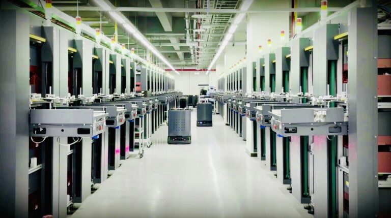
Taiwan crossed a two-layered threshold in wide-bandgap semiconductor materials on August 30, when Taisic Materials produced the island’s first 12-inch silicon carbide boule — and did so using a crystal-growth furnace designed and manufactured by its own parent company, Kenmec Mechanical Engineering. The twin achievement matters because the wafer-size record and the furnace origin tell two different strategic stories, and the furnace story is the more consequential one.
Silicon carbide doesn’t begin as a disc. Every SiC wafer starts life as a boule: a dense, cylindrical single-crystal ingot grown over days or weeks inside a high-temperature furnace using a physical vapor transport process. SiC powder is heated to between 2,000°C and 2,400°C (3,632°F and 4,352°F) inside a sealed graphite crucible, where it sublimes at pressures as low as 10–90 pascals into silicon-carbon vapor species. A carefully engineered temperature gradient — typically 10–50°C per centimeter — drives those vapors upward toward a cooler seed crystal, where they condense and grow the boule atom by atom. The process runs continuously for 100 hours or more per growth run. Every interruption degrades crystal quality.
The engineering challenge scales nonlinearly with diameter. Controlling a uniform thermal field across 12-inch crystals is an exponentially harder problem in heat-transfer physics than the 6-inch standard. The graphite crucible, the induction coil geometry, the insulation material, and the gas-flow dynamics must all be designed to hold temperature gradients within tight tolerances across an area four times larger than the 6-inch standard. This is why crystal-growth furnaces for large-diameter SiC — not the crystals they produce — represent the actual technical barrier to entry.
Growing a 12-Inch Boule Is the Milestone; Building the Furnace Is the Breakthrough
Until recently, most Asian SiC producers sourced those furnaces from the United States and Japan, the two jurisdictions that dominate precision high-temperature equipment manufacturing. In 2023, Taisic planned to operate 65 furnaces: five sourced from the US, ten from Japan, and the remainder from Kenmec. The August 30 boule changes that arithmetic. Growing a 12-inch crystal in a furnace Kenmec engineered entirely in-house means Taiwan’s SiC substrate capacity can, in principle, expand without waiting for import approvals or navigating third-country technology licensing decisions — a structural vulnerability that has drawn increasing attention as semiconductor equipment has become a flashpoint in export-control policy.
What 12 Inches Actually Means for SiC Economics
The SiC wafer market was valued at approximately $822 million in 2024 and is projected to reach $4.27 billion by 2033, growing at a compound annual growth rate of around 20 percent, driven by electric vehicle drivetrains, industrial motor drives, renewable-energy inverters, and power-delivery systems in AI data centers. SiC substrates still account for 40–50 percent of total SiC chip costs — far more than silicon substrates in conventional semiconductor production — which makes each step up in boule diameter economically transformative.
The math is straightforward: wafer area scales as the square of diameter. A 12-inch wafer has 2.25 times the surface area of an 8-inch wafer; in practice, SICC 12-inch substrate yield data shows 2.5 times more chips per wafer comparing 12-inch to 8-inch platforms. That ratio translates directly into per-device cost reduction — without requiring any improvement in the underlying growth process, just the larger canvas. Six-inch wafers dominate the market at roughly 42 percent of revenue in 2026, with 8-inch production the frontier that most manufacturers are racing to scale. Twelve-inch — Taisic’s new target — is where the industry consensus says volume production won’t arrive for even the best-resourced players until the late 2020s at the earliest.
Taisic is planting its flag in that pre-commercial terrain while the standard is still being defined.
A Decade of Deliberate Climbing
Taisic’s trajectory compresses what typically takes multinational incumbents far longer. Established less than three years before growing its first 4-inch SiC crystals, the company tripled its furnace capacity by late 2022 to supply what would become Foxconn’s 6-inch SiC fab at the Hsinchu Science Park. In June 2023, Taisic demonstrated Taiwan’s first 8-inch SiC wafer, with its chief executive noting at the time that the company’s crystal-growth technology stood approximately one year behind Wolfspeed — then the world’s only manufacturer capable of mass-producing 8-inch SiC substrates.
Foxconn (Hon Hai Precision Industry) has underpinned much of that trajectory. In July 2022, Hon Hai invested NT$500 million for a 10 percent stake in Taisic, giving the company capital and a captive demand signal. Hon Hai’s semiconductor business group president Bob Chen stated at the time that SiC substrates are “a key part of the electric vehicle supply chain, as [they account] for a large portion of overall SiC semiconductor costs.”
The vertical stack that emerged from that relationship is one of the few integrated SiC chains outside traditional Western and Japanese incumbents: Taisic handles upstream crystal growth and substrate production, Gigastorage manages wafer cutting, grinding, and polishing, and Hon Hai acquired from Macronix a SiC wafer foundry at the Hsinchu Science Park. Now Kenmec — the industrial-automation conglomerate that is Taisic’s parent — has supplied the furnace that grew Taiwan’s first 12-inch boule.
How Does SiC Crystal Growth Actually Work?
Physical vapor transport begins with high-purity SiC powder loaded into a graphite crucible, sealed inside a Kenmec-type induction furnace, and heated by radio-frequency coils to temperatures between 2,000°C and 2,400°C (3,632°F and 4,352°F). At those temperatures and pressures near vacuum, the powder sublimes into vapor species — primarily Si₂C, SiC₂, and Si — that diffuse upward through the crucible toward a SiC seed crystal mounted at the cooler top of the chamber. The seed is cooler by design; the temperature differential is what pulls vapor out of solution and drives crystal deposition.
What makes scaling to 12-inch uniquely challenging is the radial temperature uniformity problem. Across a larger seed face, thermal gradients that would be acceptable at 6-inch produce dislocations — crystal defects that degrade device performance — at 12-inch. One seed cavity simulation study found that introducing a seed-cavity design element reduced the radial temperature difference across the seed surface from 93°C (200°F) to 11°C (52°F) at 8-inch, an 88 percent improvement that enabled stable growth. Achieving comparable uniformity at 12-inch requires furnace-level thermal-field engineering that few organizations in the world have demonstrated. Kenmec’s having done it at 12-inch — and in a furnace of its own design — places it in a very short list of equipment makers capable of this class of precision.
Racing Against a Crowded Global Field
Taisic’s milestone arrives into an accelerating competitive landscape that has reordered itself significantly in the past 18 months.
The structural disruption began with Wolfspeed. The US company, which held approximately 33.7 percent of the global SiC substrate market in 2024 and was for years the only manufacturer capable of mass-producing 8-inch substrates, filed for Chapter 11 bankruptcy on June 30, 2025, burdened by $4.6 billion in debt. Wolfspeed emerged from Chapter 11 on September 29, 2025, having reduced its total debt by roughly 70 percent, and announced its own Wolfspeed 300mm SiC breakthrough on January 13, 2026. Wolfspeed Chief Technology Officer Elif Balkas described the result as “a significant technology achievement and the result of years of focused innovation in crystal growth, boule and wafer processing.”
Chinese firms moved with speed that the industry has found difficult to absorb analytically. At Semicon China in March 2025, SICC — which had already captured 22.8 percent of global SiC substrate market share in 2024 — showcased a full commercial portfolio of 12-inch substrates, including both N-type conductive and high-purity semi-insulating variants. By September 2025, JSG brought its first 12-inch pilot line online with 100 percent domestically produced core equipment. In October 2025, Zhuhai-based Tiancheng Advanced announced 12-inch HPSI SiC crystals with effective thicknesses exceeding 35 mm. December 2025 brought CGEE’s first commercial delivery of self-developed 12-inch SiC crystal furnaces. In February 2026, Roshow produced its first 12-inch single-crystal SiC sample. And in March 2026, Tiancheng Semiconductor announced a 14-inch SiC single crystal using self-developed equipment, signaling China’s intent to leapfrog the 12-inch tier entirely.
Against that backdrop, Chinese SiC market share has risen to roughly 40 percent of the global SiC substrate market, with Wolfspeed holding its position but post-bankruptcy, and Western capacity constrained by years of underinvestment relative to demand.
Kenmec’s Pivot — and What the Emerging Stock Board Listing Signals
Kenmec, founded in 1976 and listed on the Kenmec’s Taipei Exchange profile (ticker: 6125), is known primarily as an industrial-automation and factory-logistics company — automated warehousing, production-line systems, AI server liquid-cooling infrastructure. Its development of a crystal-growth furnace capable of producing 12-inch SiC boules represents a deliberate diversification into high-value semiconductor equipment, a market segment historically dominated by Japanese, German, and American players.
On August 19, Kenmec founder and president Frank Hsieh publicly confirmed the company’s ambitions for both subsidiaries via Kenmec’s Emerging Stock Board listing announcement: Taisic Materials (SiC) and a sister company called Kentec (targeting AI data-center infrastructure) are both expected to list on Taiwan’s Emerging Stock Board in October 2026. For Taiwan’s industrial policy community, the timing is meaningful: a SiC materials company and a data-center infrastructure company, both spun out of the same automation-industry parent, listing on the public market within weeks of each other, signals that the Foxconn-anchored SiC vertical is maturing toward standalone financing.
What Comes Next
Growing a single 12-inch boule and mass-producing 12-inch substrates are separated by years of process engineering: improving crystal quality, reducing dislocation densities, scaling furnace counts, qualifying wafers with device manufacturers, and bringing costs down to compete on price. Wolfspeed itself has not announced a commercialization timeline for its 300 mm platform. The 8-inch SiC ramp 2026 remains the industry priority, with 12-inch volume production still several years away for even the best-resourced players.
For Taisic, the immediate priority is likely converting the 12-inch boule demonstration into repeatable, high-yield growth runs, then advancing toward wafer qualification with power device manufacturers. Its position inside the Foxconn ecosystem provides a useful initial validation environment, though Taisic has previously signaled interest in extending substrate supply to customers outside the Hon Hai camp.
The deeper significance of August 30’s announcement may not be the 12-inch diameter at all. It may be that a Taiwanese industrial-automation company — whose primary business is warehouses and conveyor systems — designed a furnace that puts it in a category of equipment builders that most nations cannot access. That furnace is the harder thing to copy, the slower thing to acquire through import, and the more durable competitive asset. The boule it grew was Taiwan’s first 12-inch. The furnace that grew it could produce many more.
Frequently Asked Questions
Why does wafer size matter so much for silicon carbide?
Because substrate costs account for 40–50 percent of total SiC chip costs — far more than in conventional silicon semiconductor production — a larger boule diameter directly compresses per-device costs. A 12-inch (300 mm) wafer provides roughly 2.5 times more usable chip area than an 8-inch (200 mm) wafer. In a material where every growth run takes days or weeks and requires temperatures above 2,000°C (3,632°F), each size increase is a significant manufacturing efficiency gain without requiring any improvement in the underlying chemistry.
Why is the Kenmec-built furnace more strategically significant than the boule itself?
Crystal-growth furnaces for large-diameter SiC are a specialized, export-regulated equipment category dominated by US and Japanese manufacturers. Taiwan’s SiC producers — including Taisic — previously depended on importing these furnaces. As advanced semiconductor equipment has become a focus of export-control policy, dependence on foreign furnace suppliers represents a structural vulnerability: a licensing restriction or trade dispute could slow capacity expansion regardless of Taiwan’s crystal-growing expertise. A domestically designed furnace that can produce 12-inch SiC boules removes that single point of external dependency at the most technically demanding step in the process.
Who are the main competitors in the global 12-inch SiC race?
As of August 2026, the field includes Wolfspeed (US, 300 mm wafer announced January 2026, commercialization timeline unannounced), SICC (China, commercially shipping 12-inch substrates), JSG (China, pilot line online September 2025), and multiple other Chinese firms including Tiancheng and Roshow. China’s Tiancheng Semiconductor has already announced 14-inch SiC development, leapfrogging the 12-inch tier on paper. None of these players — including Wolfspeed — has announced volume production timelines; 2026 remains primarily an 8-inch scale-up year across the industry. Taisic’s distinction is the combination of the 12-inch boule and the homegrown furnace; most competitors who have achieved 12-inch results depend on some degree of imported equipment.
When can Taisic actually sell 12-inch SiC wafers at scale?
Not imminently. Moving from a single demonstrated boule to repeatable, high-yield production runs requires process engineering that typically takes years. Wafers must then qualify with device manufacturers — a qualification process that itself can take a year or more for automotive and industrial applications. Wolfspeed’s January 2026 300 mm announcement has also not been accompanied by a commercialization schedule. Volume production of 12-inch SiC substrates — by any manufacturer — is expected to be a late-2020s event. Taisic’s milestone positions it to participate in that market when it arrives; it is not a commercial announcement.